- 您現(xiàn)在的位置:買(mǎi)賣(mài)IC網(wǎng) > PDF目錄375033 > XCV812E-8FG556I (Xilinx, Inc.) Virtex-E 1.8 V Extended Memory Field Programmable Gate Arrays PDF資料下載
參數(shù)資料
| 型號(hào): | XCV812E-8FG556I |
| 廠(chǎng)商: | Xilinx, Inc. |
| 英文描述: | Virtex-E 1.8 V Extended Memory Field Programmable Gate Arrays |
| 中文描述: | 的Virtex娥內(nèi)存擴(kuò)展1.8伏現(xiàn)場(chǎng)可編程門(mén)陣列 |
| 文件頁(yè)數(shù): | 18/116頁(yè) |
| 文件大?。?/td> | 1087K |
| 代理商: | XCV812E-8FG556I |
第1頁(yè)第2頁(yè)第3頁(yè)第4頁(yè)第5頁(yè)第6頁(yè)第7頁(yè)第8頁(yè)第9頁(yè)第10頁(yè)第11頁(yè)第12頁(yè)第13頁(yè)第14頁(yè)第15頁(yè)第16頁(yè)第17頁(yè)當(dāng)前第18頁(yè)第19頁(yè)第20頁(yè)第21頁(yè)第22頁(yè)第23頁(yè)第24頁(yè)第25頁(yè)第26頁(yè)第27頁(yè)第28頁(yè)第29頁(yè)第30頁(yè)第31頁(yè)第32頁(yè)第33頁(yè)第34頁(yè)第35頁(yè)第36頁(yè)第37頁(yè)第38頁(yè)第39頁(yè)第40頁(yè)第41頁(yè)第42頁(yè)第43頁(yè)第44頁(yè)第45頁(yè)第46頁(yè)第47頁(yè)第48頁(yè)第49頁(yè)第50頁(yè)第51頁(yè)第52頁(yè)第53頁(yè)第54頁(yè)第55頁(yè)第56頁(yè)第57頁(yè)第58頁(yè)第59頁(yè)第60頁(yè)第61頁(yè)第62頁(yè)第63頁(yè)第64頁(yè)第65頁(yè)第66頁(yè)第67頁(yè)第68頁(yè)第69頁(yè)第70頁(yè)第71頁(yè)第72頁(yè)第73頁(yè)第74頁(yè)第75頁(yè)第76頁(yè)第77頁(yè)第78頁(yè)第79頁(yè)第80頁(yè)第81頁(yè)第82頁(yè)第83頁(yè)第84頁(yè)第85頁(yè)第86頁(yè)第87頁(yè)第88頁(yè)第89頁(yè)第90頁(yè)第91頁(yè)第92頁(yè)第93頁(yè)第94頁(yè)第95頁(yè)第96頁(yè)第97頁(yè)第98頁(yè)第99頁(yè)第100頁(yè)第101頁(yè)第102頁(yè)第103頁(yè)第104頁(yè)第105頁(yè)第106頁(yè)第107頁(yè)第108頁(yè)第109頁(yè)第110頁(yè)第111頁(yè)第112頁(yè)第113頁(yè)第114頁(yè)第115頁(yè)第116頁(yè)
Virtex-E 1.8 V Extended Memory Field Programmable Gate Arrays
Module 2 of 4
14
www.xilinx.com
1-800-255-7778
DS025-2 (v2.1) July 17, 2002
R
Master-Serial Mode
In master-serial mode, the CCLK output of the FPGA drives
a Xilinx Serial PROM that feeds bit-serial data to the DIN
input. The FPGA accepts this data on each rising CCLK
edge. After the FPGA has been loaded, the data for the next
device in a daisy-chain is presented on the DOUT pin after
the rising CCLK edge.
The interface is identical to slave-serial except that an inter-
nal oscillator is used to generate the configuration clock
(CCLK). A wide range of frequencies can be selected for
CCLK which always starts at a slow default frequency. Con-
figuration bits then switch CCLK to a higher frequency for
the remainder of the configuration. Switching to a lower fre-
quency is prohibited.
The CCLK frequency is set using the ConfigRate option in
the bitstream generation software. The maximum CCLK fre-
quency that can be selected is 60 MHz. When selecting a
CCLK frequency, ensure that the serial PROM and any
daisy-chained FPGAs are fast enough to support the clock
rate.
On power-up, the CCLK frequency is approximately
2.5 MHz. This frequency is used until the ConfigRate bits
have been loaded when the frequency changes to the
selected ConfigRate. Unless a different frequency is speci-
fied in the design, the default ConfigRate is 4 MHz.
Figure 13
shows a full master/slave system. In this system,
the left-most device operates in master-serial mode. The
remaining devices operate in slave-serial mode. The SPROM
RESET pin is driven by INIT, and the CE input is driven by
DONE. There is the potential for contention on the DONE pin,
depending on the start-up sequence options chosen.
The sequence of operations necessary to configure a
Virtex-E FPGA serially appears in
Figure 15
.
Figure 16
shows the timing of master-serial configuration.
Master-serial mode is selected by a <000> or <100> on the
mode pins (M2, M1, M0).
Table 10
shows the timing infor-
mation for
Figure 16
.
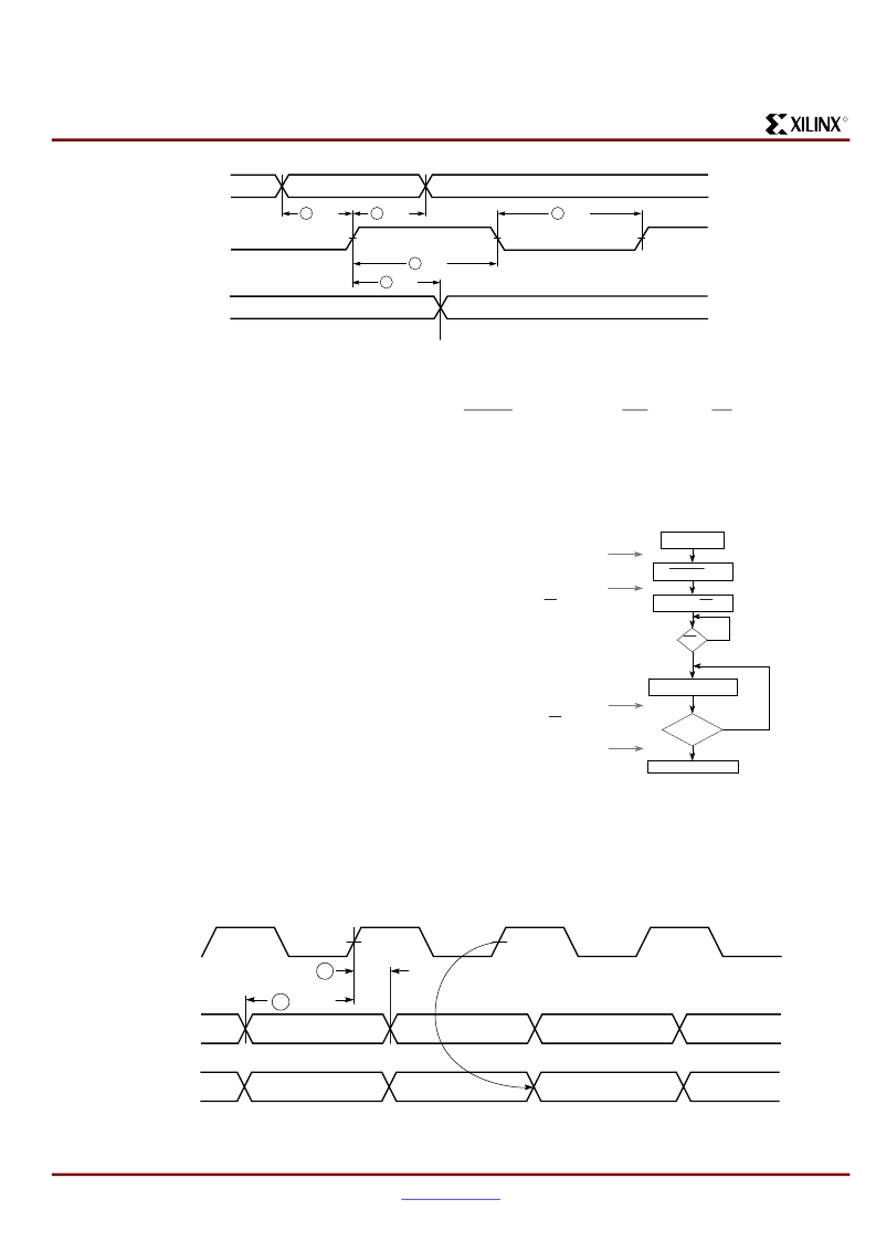
Figure 14:
Slave-Serial Mode Programming Switching Characteristics
4 T
CCH
3 T
CCO
5 T
CCL
2 T
CCD
1 T
DCC
DIN
CCLK
DOUT
(Output)
X5379_a
Figure 15:
Serial Configuration Flowchart
Apply Power
Set PROGRAM = High
Release INIT
If used to delay
Load a Configuration Bit
High
Low
FPGA makes a final
clearing pass and releases
INIT when finished.
FPGA starts to clear
configuration memory.
ds009_15_111799
Configuration Completed
BiEnd of
Yes
No
Once per bitstream,
FPGA checks data using CRC
and pulls INIT Low on error.
If no CRC errors found,
FPGA enters start-up phase
causing DONE to go High.
INIT
Figure 16:
Master-Serial Mode Programming Switching Characteristics
Serial Data In
CCLK
(Output)
Serial DOUT
(Output)
1 TDSCK
2
TCKDS
DS022_44_071201
相關(guān)PDF資料 |
PDF描述 |
|---|---|
| XCV812E-8FG560C | Virtex-E 1.8 V Extended Memory Field Programmable Gate Arrays |
| XCV812E-8FG560I | Virtex-E 1.8 V Extended Memory Field Programmable Gate Arrays |
| XCV812E-8FG676C | Virtex-E 1.8 V Extended Memory Field Programmable Gate Arrays |
| XCV812E-8FG676I | Virtex-E 1.8 V Extended Memory Field Programmable Gate Arrays |
| XCV812E-8FG900C | Virtex-E 1.8 V Extended Memory Field Programmable Gate Arrays |
相關(guān)代理商/技術(shù)參數(shù) |
參數(shù)描述 |
|---|---|
| XCV812E-8FG560C | 制造商:XILINX 制造商全稱(chēng):XILINX 功能描述:Virtex-E 1.8 V Extended Memory Field Programmable Gate Arrays |
| XCV812E-8FG560I | 制造商:XILINX 制造商全稱(chēng):XILINX 功能描述:Virtex-E 1.8 V Extended Memory Field Programmable Gate Arrays |
| XCV812E-8FG676C | 制造商:XILINX 制造商全稱(chēng):XILINX 功能描述:Virtex-E 1.8 V Extended Memory Field Programmable Gate Arrays |
| XCV812E-8FG676I | 制造商:XILINX 制造商全稱(chēng):XILINX 功能描述:Virtex-E 1.8 V Extended Memory Field Programmable Gate Arrays |
| XCV812E-8FG900C | 功能描述:IC FPGA 1.8V C-TEMP 900-FBGA RoHS:否 類(lèi)別:集成電路 (IC) >> 嵌入式 - FPGA(現(xiàn)場(chǎng)可編程門(mén)陣列) 系列:Virtex®-E EM 產(chǎn)品變化通告:XC4000(E,L) Discontinuation 01/April/2002 標(biāo)準(zhǔn)包裝:24 系列:XC4000E/X LAB/CLB數(shù):100 邏輯元件/單元數(shù):238 RAM 位總計(jì):3200 輸入/輸出數(shù):80 門(mén)數(shù):3000 電源電壓:4.5 V ~ 5.5 V 安裝類(lèi)型:表面貼裝 工作溫度:-40°C ~ 100°C 封裝/外殼:120-BCBGA 供應(yīng)商設(shè)備封裝:120-CPGA(34.55x34.55) |
發(fā)布緊急采購(gòu),3分鐘左右您將得到回復(fù)。