- 您現(xiàn)在的位置:買賣IC網(wǎng) > PDF目錄375033 > XCV812E-8BG900C (Xilinx, Inc.) Virtex-E 1.8 V Extended Memory Field Programmable Gate Arrays PDF資料下載
參數(shù)資料
| 型號(hào): | XCV812E-8BG900C |
| 廠商: | Xilinx, Inc. |
| 英文描述: | Virtex-E 1.8 V Extended Memory Field Programmable Gate Arrays |
| 中文描述: | 的Virtex娥內(nèi)存擴(kuò)展1.8伏現(xiàn)場(chǎng)可編程門陣列 |
| 文件頁(yè)數(shù): | 7/116頁(yè) |
| 文件大小: | 1087K |
| 代理商: | XCV812E-8BG900C |
第1頁(yè)第2頁(yè)第3頁(yè)第4頁(yè)第5頁(yè)第6頁(yè)當(dāng)前第7頁(yè)第8頁(yè)第9頁(yè)第10頁(yè)第11頁(yè)第12頁(yè)第13頁(yè)第14頁(yè)第15頁(yè)第16頁(yè)第17頁(yè)第18頁(yè)第19頁(yè)第20頁(yè)第21頁(yè)第22頁(yè)第23頁(yè)第24頁(yè)第25頁(yè)第26頁(yè)第27頁(yè)第28頁(yè)第29頁(yè)第30頁(yè)第31頁(yè)第32頁(yè)第33頁(yè)第34頁(yè)第35頁(yè)第36頁(yè)第37頁(yè)第38頁(yè)第39頁(yè)第40頁(yè)第41頁(yè)第42頁(yè)第43頁(yè)第44頁(yè)第45頁(yè)第46頁(yè)第47頁(yè)第48頁(yè)第49頁(yè)第50頁(yè)第51頁(yè)第52頁(yè)第53頁(yè)第54頁(yè)第55頁(yè)第56頁(yè)第57頁(yè)第58頁(yè)第59頁(yè)第60頁(yè)第61頁(yè)第62頁(yè)第63頁(yè)第64頁(yè)第65頁(yè)第66頁(yè)第67頁(yè)第68頁(yè)第69頁(yè)第70頁(yè)第71頁(yè)第72頁(yè)第73頁(yè)第74頁(yè)第75頁(yè)第76頁(yè)第77頁(yè)第78頁(yè)第79頁(yè)第80頁(yè)第81頁(yè)第82頁(yè)第83頁(yè)第84頁(yè)第85頁(yè)第86頁(yè)第87頁(yè)第88頁(yè)第89頁(yè)第90頁(yè)第91頁(yè)第92頁(yè)第93頁(yè)第94頁(yè)第95頁(yè)第96頁(yè)第97頁(yè)第98頁(yè)第99頁(yè)第100頁(yè)第101頁(yè)第102頁(yè)第103頁(yè)第104頁(yè)第105頁(yè)第106頁(yè)第107頁(yè)第108頁(yè)第109頁(yè)第110頁(yè)第111頁(yè)第112頁(yè)第113頁(yè)第114頁(yè)第115頁(yè)第116頁(yè)
Virtex-E 1.8 V Extended Memory Field Programmable Gate Arrays
DS025-2 (v2.1) July 17, 2002
www.xilinx.com
1-800-255-7778
Module 2 of 4
3
R
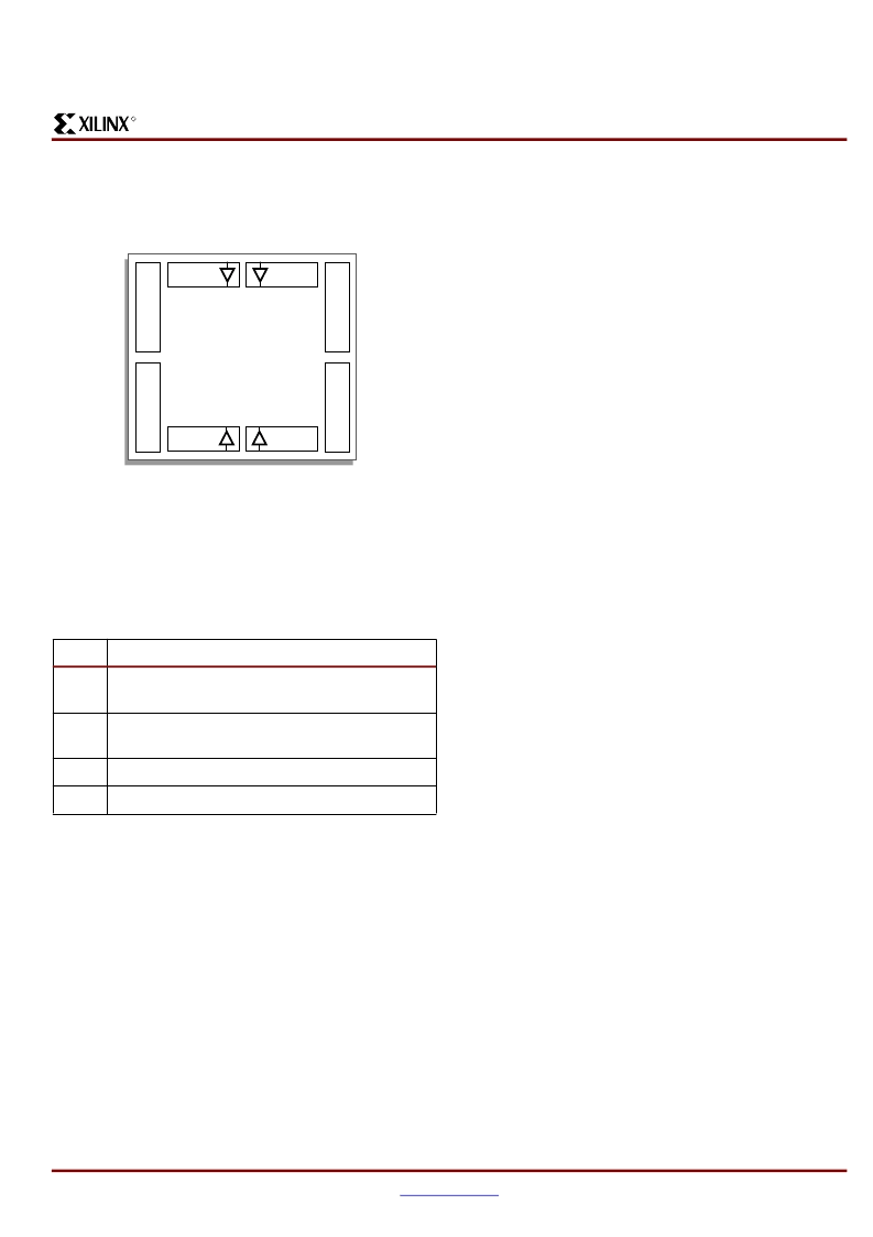
Eight I/O banks result from separating each edge of the
FPGA into two banks, as shown in
Figure 3
. Each bank has
multiple V
CCO
pins, all of which must be connected to the
same voltage. This voltage is determined by the output
standards in use.
Within a bank, output standards can be mixed only if they
use the same V
CCO
. Compatible standards are shown in
Table 2
. GTL and GTL+ appear under all voltages because
their open-drain outputs do not depend on V
CCO
.
Some input standards require a user-supplied threshold
voltage, V
REF
. In this case, certain user-I/O pins are auto-
matically configured as inputs for the V
REF
voltage. Approx-
imately one in six of the I/O pins in the bank assume this
role.
The V
REF
pins within a bank are interconnected internally
and consequently only one V
REF
voltage can be used within
each bank. All V
REF
pins in the bank, however, must be con-
nected to the external voltage source for correct operation.
Within a bank, inputs that require V
REF
can be mixed with
those that do not. However, only one V
REF
voltage can be
used within a bank.
In Virtex-E, input buffers with LVTTL, LVCMOS2,
LVCMOS18, PCI33_3, PCI66_3 standards are supplied by
V
CCO
rather than V
CCINT
. For these standards, only input
and output buffers that have the same V
CCO
can be mixed
together.
The V
CCO
and V
REF
pins for each bank appear in the device
pin-out tables and diagrams. The diagrams also show the
bank affiliation of each I/O.
Within a given package, the number of V
REF
and V
CCO
pins
can vary depending on the size of device. In larger devices,
more I/O pins convert to V
REF
pins. Since these are always
a super set of the V
REF
pins used for smaller devices, it is
possible to design a PCB that permits migration to a larger
device if necessary. All the V
REF
pins for the largest device
anticipated must be connected to the V
REF
voltage, and not
used for I/O.
In smaller devices, some V
CCO
pins used in larger devices
do not connect within the package. These unconnected pins
can be left unconnected externally, or they can be con-
nected to the V
CCO
voltage to permit migration to a larger
device, if necessary.
Configurable Logic Block
The basic building block of the Virtex-E CLB is the logic cell
(LC). An LC includes a 4-input function generator, carry
logic, and a storage element. The output from the function
generator in each LC drives both the CLB output and the D
input of the flip-flop. Each Virtex-E CLB contains four LCs,
organized in two similar slices, as shown in
Figure 4
.
Figure 5
shows a more detailed view of a single slice.
Figure 3:
Virtex-E I/O Banks
Table 2:
Compatible Output Standards
V
CCO
Compatible Standards
3.3 V
PCI, LVTTL, SSTL3 I, SSTL3 II, CTT, AGP, GTL,
GTL+, LVPECL
2.5 V
SSTL2 I, SSTL2 II, LVCMOS2, GTL, GTL+,
BLVDS, LVDS
1.8 V
LVCMOS18, GTL, GTL+
1.5 V
HSTL I, HSTL III, HSTL IV, GTL, GTL+
ds022_03_121799
Bank 0
GCLK3 GCLK2
GCLK1 GCLK0
Bank 1
Bank 5
Bank 4
VirtexE
Device
B
B
B
B
相關(guān)PDF資料 |
PDF描述 |
|---|---|
| XCV812E-8BG900I | Virtex-E 1.8 V Extended Memory Field Programmable Gate Arrays |
| XCV812E-8FG404C | Virtex-E 1.8 V Extended Memory Field Programmable Gate Arrays |
| XCV812E-8FG404I | Virtex-E 1.8 V Extended Memory Field Programmable Gate Arrays |
| XCV812E-8FG556C | Virtex-E 1.8 V Extended Memory Field Programmable Gate Arrays |
| XCV812E-8FG556I | Virtex-E 1.8 V Extended Memory Field Programmable Gate Arrays |
相關(guān)代理商/技術(shù)參數(shù) |
參數(shù)描述 |
|---|---|
| XCV812E-8BG900I | 制造商:XILINX 制造商全稱:XILINX 功能描述:Virtex-E 1.8 V Extended Memory Field Programmable Gate Arrays |
| XCV812E-8FG404C | 制造商:XILINX 制造商全稱:XILINX 功能描述:Virtex-E 1.8 V Extended Memory Field Programmable Gate Arrays |
| XCV812E-8FG404I | 制造商:XILINX 制造商全稱:XILINX 功能描述:Virtex-E 1.8 V Extended Memory Field Programmable Gate Arrays |
| XCV812E-8FG556C | 制造商:XILINX 制造商全稱:XILINX 功能描述:Virtex-E 1.8 V Extended Memory Field Programmable Gate Arrays |
| XCV812E-8FG556I | 制造商:XILINX 制造商全稱:XILINX 功能描述:Virtex-E 1.8 V Extended Memory Field Programmable Gate Arrays |
發(fā)布緊急采購(gòu),3分鐘左右您將得到回復(fù)。