- 您現(xiàn)在的位置:買賣IC網(wǎng) > PDF目錄375033 > XCV812E-6FG404C (Xilinx, Inc.) Virtex-E 1.8 V Extended Memory Field Programmable Gate Arrays PDF資料下載
參數(shù)資料
| 型號(hào): | XCV812E-6FG404C |
| 廠商: | Xilinx, Inc. |
| 英文描述: | Virtex-E 1.8 V Extended Memory Field Programmable Gate Arrays |
| 中文描述: | 的Virtex娥內(nèi)存擴(kuò)展1.8伏現(xiàn)場(chǎng)可編程門陣列 |
| 文件頁數(shù): | 17/116頁 |
| 文件大小: | 1087K |
| 代理商: | XCV812E-6FG404C |
第1頁第2頁第3頁第4頁第5頁第6頁第7頁第8頁第9頁第10頁第11頁第12頁第13頁第14頁第15頁第16頁當(dāng)前第17頁第18頁第19頁第20頁第21頁第22頁第23頁第24頁第25頁第26頁第27頁第28頁第29頁第30頁第31頁第32頁第33頁第34頁第35頁第36頁第37頁第38頁第39頁第40頁第41頁第42頁第43頁第44頁第45頁第46頁第47頁第48頁第49頁第50頁第51頁第52頁第53頁第54頁第55頁第56頁第57頁第58頁第59頁第60頁第61頁第62頁第63頁第64頁第65頁第66頁第67頁第68頁第69頁第70頁第71頁第72頁第73頁第74頁第75頁第76頁第77頁第78頁第79頁第80頁第81頁第82頁第83頁第84頁第85頁第86頁第87頁第88頁第89頁第90頁第91頁第92頁第93頁第94頁第95頁第96頁第97頁第98頁第99頁第100頁第101頁第102頁第103頁第104頁第105頁第106頁第107頁第108頁第109頁第110頁第111頁第112頁第113頁第114頁第115頁第116頁
Virtex-E 1.8 V Extended Memory Field Programmable Gate Arrays
DS025-2 (v2.1) July 17, 2002
www.xilinx.com
1-800-255-7778
Module 2 of 4
13
R
Table 9
lists the total number of bits required to configure
each device.
Slave-Serial Mode
In slave-serial mode, the FPGA receives configuration data
in bit-serial form from a serial PROM or other source of
serial configuration data. The serial bitstream must be set
up at the DIN input pin a short time before each rising edge
of an externally generated CCLK.
For more information on serial PROMs, see the PROM data
sheet at
http://www.xilinx.com/partinfo/ds026.pdf
.
Multiple FPGAs can be daisy-chained for configuration from
a single source. After a particular FPGA has been config-
ured, the data for the next device is routed to the DOUT pin.
Data on the DOUT pin changes on the rising edge of CCLK.
The change of DOUT on the rising edge of CCLK differs
from previous families but does not cause a problem for
mixed configuration chains. This change was made to
improve serial configuration rates for Virtex and Virtex-E
only chains.
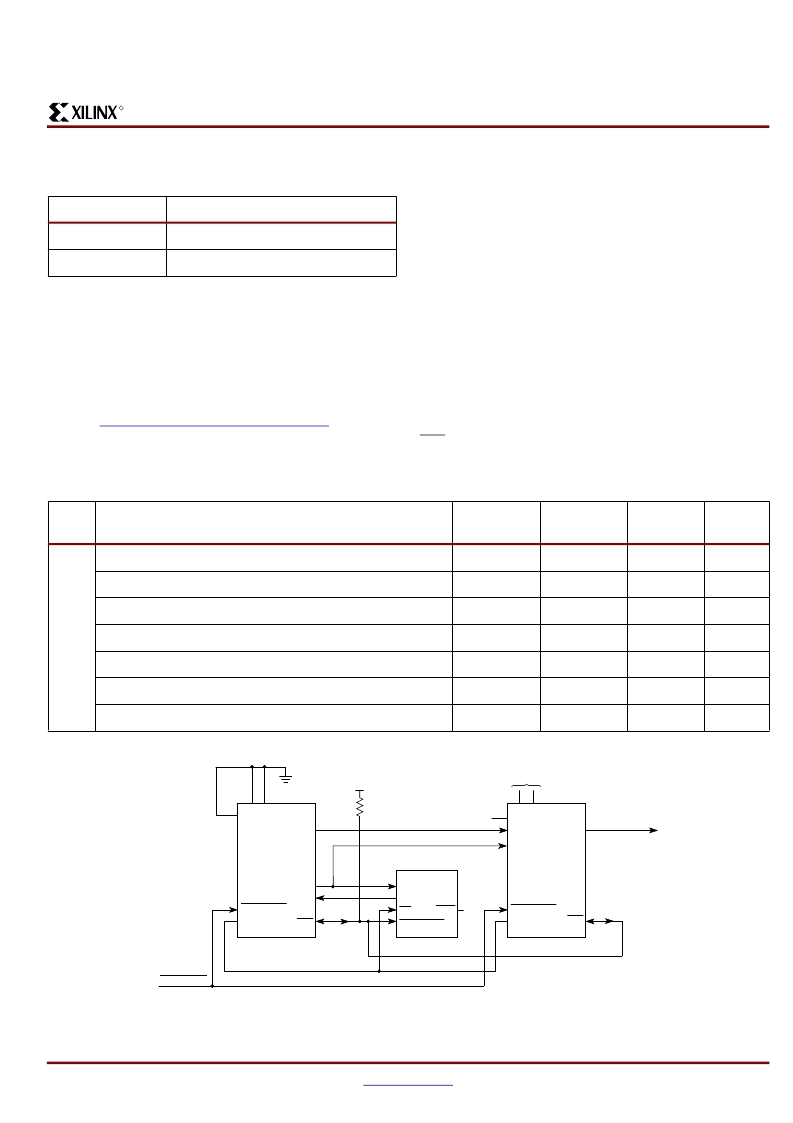
Figure 13
shows a full master/slave system. A Virtex-E
device in slave-serial mode should be connected as shown
in the right-most device.
Slave-serial mode is selected by applying <111> or <011>
to the mode pins (M2, M1, M0). A weak pull-up on the mode
pins makes slave-serial the default mode if the pins are left
unconnected.
Figure 14
shows slave-serial configuration
timing.
Table 10
provides more detail about the characteristics
shown in
Figure 14
. Configuration must be delayed until the
INIT pins of all daisy-chained FPGAs are High.
Table 9:
Virtex-E Bitstream Lengths
Device
# of Configuration Bits
XCV405E
3,430,400
XCV812E
6,519,648
Table 10:
Master/Slave Serial Mode Programming Switching
Description
Figure
References
Symbol
Values
Units
CCLK
DIN setup/hold, slave mode
1/2
T
DCC
/T
CCD
5.0/0.0
ns, min
DIN setup/hold, master mode
1/2
T
DSCK
/T
CKDS
5.0/0.0
ns, min
DOUT
3
T
CCO
12.0
ns, max
High time
4
T
CCH
5.0
ns, min
Low time
5
T
CCL
5.0
ns, min
Maximum Frequency
F
CC
66
MHz, max
Frequency Tolerance, master mode with respect to nominal
+45% –30%
Figure 13:
Master/Slave Serial Mode Circuit Diagram
VIRTEX-E
MASTER
SERIAL
VIRTEX-E,
XC4000XL,
SLAVE
XC1701L
PROGRAM
M2
M0 M1
DOUT
CCLK
DIN
CLK
DATA
CE
RESET/OE
3.3V
CEO
DONE
INIT
INIT
DONE
PROGRAM
PROGRAM
CCLK
DIN
DOUT
M2
M0 M1
(Low Reset Option Used)
4.7 K
XCVE_ds_013
N/C
N/C
相關(guān)PDF資料 |
PDF描述 |
|---|---|
| XCV812E-6FG404I | Virtex-E 1.8 V Extended Memory Field Programmable Gate Arrays |
| XCV812E-6FG556C | Virtex-E 1.8 V Extended Memory Field Programmable Gate Arrays |
| XCV812E-6FG556I | Virtex-E 1.8 V Extended Memory Field Programmable Gate Arrays |
| XCV812E-6FG560C | Virtex-E 1.8 V Extended Memory Field Programmable Gate Arrays |
| XCV812E-6FG560I | Virtex-E 1.8 V Extended Memory Field Programmable Gate Arrays |
相關(guān)代理商/技術(shù)參數(shù) |
參數(shù)描述 |
|---|---|
| XCV812E-6FG404I | 制造商:XILINX 制造商全稱:XILINX 功能描述:Virtex-E 1.8 V Extended Memory Field Programmable Gate Arrays |
| XCV812E-6FG556C | 制造商:XILINX 制造商全稱:XILINX 功能描述:Virtex-E 1.8 V Extended Memory Field Programmable Gate Arrays |
| XCV812E-6FG556I | 制造商:XILINX 制造商全稱:XILINX 功能描述:Virtex-E 1.8 V Extended Memory Field Programmable Gate Arrays |
| XCV812E-6FG560C | 制造商:XILINX 制造商全稱:XILINX 功能描述:Virtex-E 1.8 V Extended Memory Field Programmable Gate Arrays |
| XCV812E-6FG560I | 制造商:XILINX 制造商全稱:XILINX 功能描述:Virtex-E 1.8 V Extended Memory Field Programmable Gate Arrays |
發(fā)布緊急采購,3分鐘左右您將得到回復(fù)。