- 您現(xiàn)在的位置:買賣IC網(wǎng) > PDF目錄375033 > XCV812E-6BG676C (Xilinx, Inc.) Virtex-E 1.8 V Extended Memory Field Programmable Gate Arrays PDF資料下載
參數(shù)資料
| 型號: | XCV812E-6BG676C |
| 廠商: | Xilinx, Inc. |
| 英文描述: | Virtex-E 1.8 V Extended Memory Field Programmable Gate Arrays |
| 中文描述: | 的Virtex娥內(nèi)存擴(kuò)展1.8伏現(xiàn)場可編程門陣列 |
| 文件頁數(shù): | 14/116頁 |
| 文件大?。?/td> | 1087K |
| 代理商: | XCV812E-6BG676C |
第1頁第2頁第3頁第4頁第5頁第6頁第7頁第8頁第9頁第10頁第11頁第12頁第13頁當(dāng)前第14頁第15頁第16頁第17頁第18頁第19頁第20頁第21頁第22頁第23頁第24頁第25頁第26頁第27頁第28頁第29頁第30頁第31頁第32頁第33頁第34頁第35頁第36頁第37頁第38頁第39頁第40頁第41頁第42頁第43頁第44頁第45頁第46頁第47頁第48頁第49頁第50頁第51頁第52頁第53頁第54頁第55頁第56頁第57頁第58頁第59頁第60頁第61頁第62頁第63頁第64頁第65頁第66頁第67頁第68頁第69頁第70頁第71頁第72頁第73頁第74頁第75頁第76頁第77頁第78頁第79頁第80頁第81頁第82頁第83頁第84頁第85頁第86頁第87頁第88頁第89頁第90頁第91頁第92頁第93頁第94頁第95頁第96頁第97頁第98頁第99頁第100頁第101頁第102頁第103頁第104頁第105頁第106頁第107頁第108頁第109頁第110頁第111頁第112頁第113頁第114頁第115頁第116頁
Virtex-E 1.8 V Extended Memory Field Programmable Gate Arrays
Module 2 of 4
10
www.xilinx.com
1-800-255-7778
DS025-2 (v2.1) July 17, 2002
R
Instruction Set
The Virtex-E Series boundary scan instruction set also
includes instructions to configure the device and read back
configuration data (CFG_IN, CFG_OUT, and JSTART). The
complete instruction set is coded as shown in
Table 6
.
Data Registers
The primary data register is the boundary scan register. For
each IOB pin in the FPGA, bonded or not, it includes three
bits for In, Out, and 3-State Control. Non-IOB pins have
appropriate partial bit population if input-only or output-only.
Each EXTEST CAPTURED-OR state captures all In, Out,
and 3-state pins.
The other standard data register is the single flip-flop
BYPASS register. It synchronizes data being passed
through the FPGA to the next downstream boundary scan
device.
The FPGA supports up to two additional internal scan
chains that can be specified using the BSCAN macro. The
macro provides two user pins (SEL1 and SEL2) which are
decodes of the USER1 and USER2 instructions respec-
tively. For these instructions, two corresponding pins (T
DO1 and TDO2) allow user scan data to be shifted out of
TDO.
Likewise, there are individual clock pins (DRCK1 and
DRCK2) for each user register. There is a common input pin
(TDI) and shared output pins that represent the state of the
TAP controller (RESET, SHIFT, and UPDATE).
Bit Sequence
The order within each IOB is: In, Out, 3-State. The
input-only pins contribute only the In bit to the boundary
scan I/O data register, while the output-only pins contributes
all three bits.
From a cavity-up view of the chip (as shown in EPIC), start-
ing in the upper right chip corner, the boundary scan
data-register bits are ordered as shown in
Figure 12
.
BSDL (Boundary Scan Description Language) files for Vir-
tex-E Series devices are available on the Xilinx web site in
the File Download area.
Table 6:
Boundary Scan Instructions
Boundary-Scan
Command
Binary
Code (4:0)
Description
EXTEST
00000
Enable boundary-scan
EXTEST operation.
SAMPLE/
PRELOAD
00001
Enable boundary-scan
SAMPLE/PRELOAD
operation.
USER1
00010
Access user-defined
register 1.
USER2
00011
Access user-defined
register 2.
CFG_OUT
00100
Access the
configuration bus for
read operations.
CFG_IN
00101
Access the
configuration bus for
write operations.
INTEST
00111
Enable boundary-scan
INTEST operation.
USERCODE
01000
Enable shifting out
USER code.
IDCODE
01001
Enable shifting out of ID
Code.
HIGHZ
01010
3-state output pins while
enabling the Bypass
Register.
JSTART
01100
Clock the start-up
sequence when
StartupClk is TCK.
BYPASS
11111
Enable BYPASS.
RESERVED
All other
codes
Xilinx reserved
instructions.
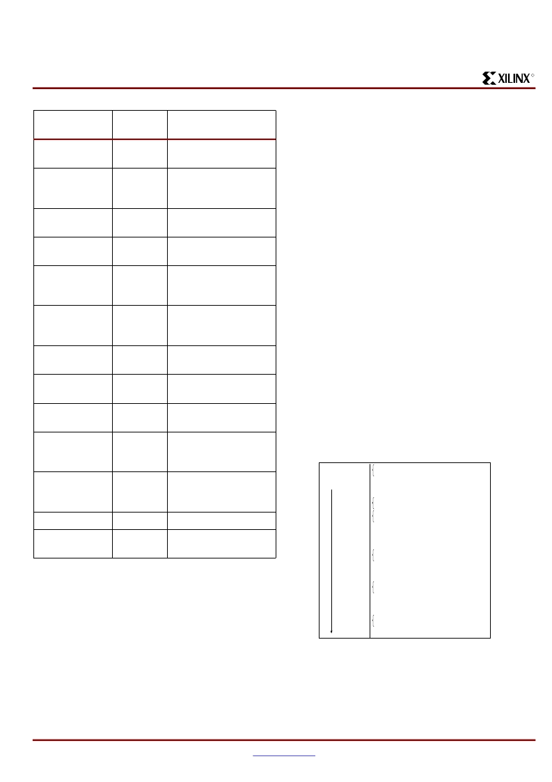
Figure 12:
Boundary Scan Bit Sequence
Bit 0 ( TDO end)
Bit 1
Bit 2
Right half of top-edge IOBs (Right to Left)
GCLK2
GCLK3
Left half of top-edge IOBs (Right to Left)
Left-edge IOBs (Top to Bottom)
M1
M0
M2
Left half of bottom-edge IOBs (Left to Right)
GCLK1
GCLK0
Right half of bottom-edge IOBs (Left to Right)
DONE
PROG
Right-edge IOBs (Bottom to Top)
CCLK
(TDI end)
990602001
相關(guān)PDF資料 |
PDF描述 |
|---|---|
| XCV812E-6BG676I | Virtex-E 1.8 V Extended Memory Field Programmable Gate Arrays |
| XCV812E-6BG900C | Virtex-E 1.8 V Extended Memory Field Programmable Gate Arrays |
| XCV812E-6BG900I | Virtex-E 1.8 V Extended Memory Field Programmable Gate Arrays |
| XCV812E-6FG404C | Virtex-E 1.8 V Extended Memory Field Programmable Gate Arrays |
| XCV812E-6FG404I | Virtex-E 1.8 V Extended Memory Field Programmable Gate Arrays |
相關(guān)代理商/技術(shù)參數(shù) |
參數(shù)描述 |
|---|---|
| XCV812E-6BG676I | 制造商:XILINX 制造商全稱:XILINX 功能描述:Virtex-E 1.8 V Extended Memory Field Programmable Gate Arrays |
| XCV812E-6BG900C | 制造商:XILINX 制造商全稱:XILINX 功能描述:Virtex-E 1.8 V Extended Memory Field Programmable Gate Arrays |
| XCV812E-6BG900I | 制造商:XILINX 制造商全稱:XILINX 功能描述:Virtex-E 1.8 V Extended Memory Field Programmable Gate Arrays |
| XCV812E-6FG404C | 制造商:XILINX 制造商全稱:XILINX 功能描述:Virtex-E 1.8 V Extended Memory Field Programmable Gate Arrays |
| XCV812E-6FG404I | 制造商:XILINX 制造商全稱:XILINX 功能描述:Virtex-E 1.8 V Extended Memory Field Programmable Gate Arrays |
發(fā)布緊急采購,3分鐘左右您將得到回復(fù)。