- 您現(xiàn)在的位置:買賣IC網(wǎng) > PDF目錄375001 > XC5202-6PQ160C (Xilinx, Inc.) Field Programmable Gate Arrays PDF資料下載
參數(shù)資料
| 型號: | XC5202-6PQ160C |
| 廠商: | Xilinx, Inc. |
| 英文描述: | Field Programmable Gate Arrays |
| 中文描述: | 現(xiàn)場可編程門陣列 |
| 文件頁數(shù): | 47/73頁 |
| 文件大小: | 598K |
| 代理商: | XC5202-6PQ160C |
第1頁第2頁第3頁第4頁第5頁第6頁第7頁第8頁第9頁第10頁第11頁第12頁第13頁第14頁第15頁第16頁第17頁第18頁第19頁第20頁第21頁第22頁第23頁第24頁第25頁第26頁第27頁第28頁第29頁第30頁第31頁第32頁第33頁第34頁第35頁第36頁第37頁第38頁第39頁第40頁第41頁第42頁第43頁第44頁第45頁第46頁當(dāng)前第47頁第48頁第49頁第50頁第51頁第52頁第53頁第54頁第55頁第56頁第57頁第58頁第59頁第60頁第61頁第62頁第63頁第64頁第65頁第66頁第67頁第68頁第69頁第70頁第71頁第72頁第73頁
R
November 5, 1998 (Version 5.2)
7-129
XC5200 Series Field Programmable Gate Arrays
7
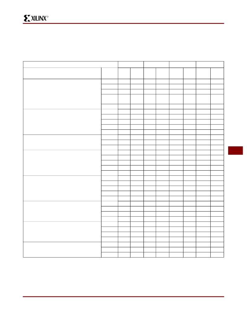
XC5200 CLB Switching Characteristic Guidelines
Testing of the switching parameters is modeled after testing methods specified by MIL-M-38510/605. All devices are 100%
functionally tested. Since many internal timing parameters cannot be measured directly, they are derived from benchmark
timing patterns. The following guidelines reflect worst-case values over the recommended operating conditions. For more
detailed, more precise, and more up-to-date timing information, use the values provided by the timing calculator and used
in the simulator.
Speed Grade
-6
-5
-4
-3
Description
Symbol
Min
(ns)
Max
(ns)
Min
(ns)
Max
(ns)
Min
(ns)
Max
(ns)
Min
(ns)
Max
(ns)
Combinatorial Delays
F inputs to X output
F inputs via transparent latch to Q
DI inputs to DO output (Logic-Cell
Feedthrough)
F inputs via F5_MUX to DO output
Carry Delays
Incremental delay per bit
Carry-in overhead from DI
Carry-in overhead from F
Carry-out overhead to DO
Sequential Delays
Clock (CK) to out (Q) (Flip-Flop)
Gate (Latch enable) going active to out (Q)
Set-up Time Before Clock (CK)
F inputs
F inputs via F5_MUX
DI input
CE input
Hold Times After Clock (CK)
F inputs
F inputs via F5_MUX
DI input
CE input
Clock Widths
Clock High Time
Clock Low Time
Toggle Frequency (MHz) (Note 3)
Reset Delays
Width (High)
Delay from CLR to Q (Flip-Flop)
Delay from CLR to Q (Latch)
Global Reset Delays
Width (High)
Delay from internal GR to Q
T
ILO
T
ITO
T
IDO
5.6
8.0
4.3
4.6
6.6
3.5
3.8
5.4
2.8
3.0
4.3
2.4
T
IMO
7.2
5.8
5.0
4.3
T
CY
T
CYDI
T
CYL
T
CYO
0.7
1.8
3.7
4.0
0.6
1.6
3.2
3.2
0.5
1.5
2.9
2.5
0.5
1.4
2.4
2.1
T
CKO
T
GO
5.8
9.2
4.9
7.4
4.0
5.9
4.0
5.5
T
ICK
T
MICK
T
DICK
T
EICK
2.3
3.8
0.8
1.6
1.8
3.0
0.5
1.2
1.4
2.5
0.4
0.9
1.3
2.4
0.4
0.9
T
CKI
T
CKMI
T
CKDI
T
CKEI
0
0
0
0
0
0
0
0
0
0
0
0
0
0
0
0
T
CH
T
CL
F
TOG
6.0
6.0
6.0
6.0
6.0
6.0
6.0
6.0
83
83
83
83
T
CLRW
T
CLR
T
CLRL
6.0
6.0
6.0
6.0
7.7
6.5
6.3
5.2
5.1
4.2
4.0
3.0
T
GCLRW
T
GCLR
6.0
6.0
6.0
6.0
14.7
12.1
9.1
8.0
Note:
1. The CLB K to Q output delay (T
CKO
) of any CLB, plus the shortest possible interconnect delay, is always longer than the
Data In hold-time requirement (T
) of any CLB on the same die.
2. Timing is based upon the XC5215 device. For other devices, see Timing Calculator.
3. Maximum flip-flop toggle rate for export control purposes.
相關(guān)PDF資料 |
PDF描述 |
|---|---|
| XC68341CFT16 | Integrated Processor Users Manual |
| XC68341CFT25 | Integrated Processor Users Manual |
| XC68341FT16 | Integrated Processor Users Manual |
| XC68341FT16V | Integrated Processor Users Manual |
| XC68341FT25 | Integrated Processor Users Manual |
相關(guān)代理商/技術(shù)參數(shù) |
參數(shù)描述 |
|---|---|
| XC5202-6PQ208C | 制造商:XILINX 制造商全稱:XILINX 功能描述:Field Programmable Gate Arrays |
| XC5202-6PQ240C | 制造商:XILINX 制造商全稱:XILINX 功能描述:Field Programmable Gate Arrays |
| XC5202-6TQ144C | 制造商:XILINX 制造商全稱:XILINX 功能描述:Field Programmable Gate Arrays |
| XC5202-6TQ176C | 制造商:XILINX 制造商全稱:XILINX 功能描述:Field Programmable Gate Arrays |
| XC5202-6VQ10 | 制造商:Xilinx 功能描述: |
發(fā)布緊急采購,3分鐘左右您將得到回復(fù)。