- 您現在的位置:買賣IC網 > PDF目錄375001 > XC5202-6PC84C (XILINX INC) Field Programmable Gate Arrays PDF資料下載
參數資料
| 型號: | XC5202-6PC84C |
| 廠商: | XILINX INC |
| 元件分類: | FPGA |
| 英文描述: | Field Programmable Gate Arrays |
| 中文描述: | FPGA, 64 CLBS, 2000 GATES, 83 MHz, PQCC84 |
| 封裝: | PLASTIC, LCC-84 |
| 文件頁數: | 9/73頁 |
| 文件大?。?/td> | 598K |
| 代理商: | XC5202-6PC84C |
第1頁第2頁第3頁第4頁第5頁第6頁第7頁第8頁當前第9頁第10頁第11頁第12頁第13頁第14頁第15頁第16頁第17頁第18頁第19頁第20頁第21頁第22頁第23頁第24頁第25頁第26頁第27頁第28頁第29頁第30頁第31頁第32頁第33頁第34頁第35頁第36頁第37頁第38頁第39頁第40頁第41頁第42頁第43頁第44頁第45頁第46頁第47頁第48頁第49頁第50頁第51頁第52頁第53頁第54頁第55頁第56頁第57頁第58頁第59頁第60頁第61頁第62頁第63頁第64頁第65頁第66頁第67頁第68頁第69頁第70頁第71頁第72頁第73頁
R
November 5, 1998 (Version 5.2)
7-91
XC5200 Series Field Programmable Gate Arrays
7
Input/Output Blocks
User-configurable input/output blocks (IOBs) provide the
interface between external package pins and the internal
logic. Each IOB controls one package pin and can be con-
figured for input, output, or bidirectional signals.
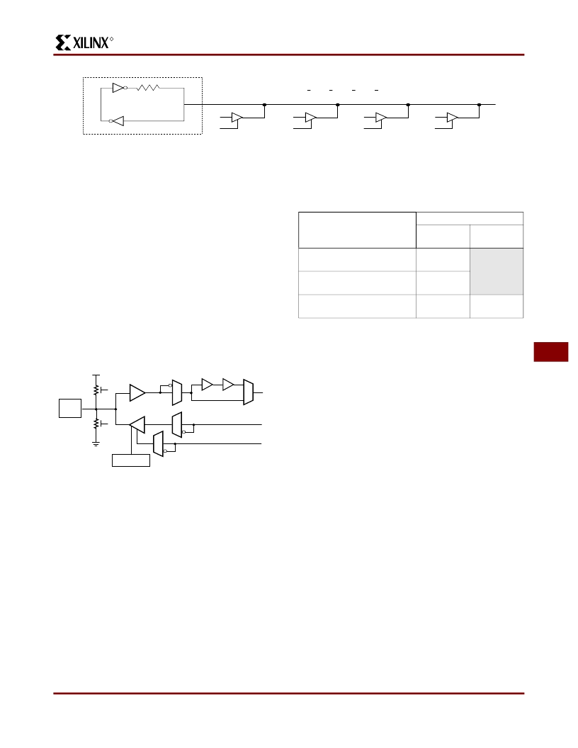
The I/O block, shown in
Figure 11
, consists of an input
buffer and an output buffer. The output driver is an 8-mA
full-rail CMOS buffer with 3-state control. Two slew-rate
control modes are supported to minimize bus transients.
Both the output buffer and the 3-state control are invertible.
The input buffer has globally selected CMOS or TTL input
thresholds. The input buffer is invertible and also provides a
programmable delay line to assure reliable chip-to-chip
set-up and hold times. Minimum ESD protection is 3 KV
using the Human Body Model.
IOB Input Signals
The XC5200 inputs can be globally configured for either
TTL (1.2V) or CMOS thresholds, using an option in the bit-
stream generation software. There is a slight hysteresis of
about 300mV.
The inputs of XC5200-Series 5-Volt devices can be driven
by the outputs of any 3.3-Volt device, if the 5-Volt inputs are
in TTL mode.
Supported sources for XC5200-Series device inputs are
shown in
Table 5
.
Optional Delay Guarantees Zero Hold Time
XC5200 devices do not have storage elements in the IOBs.
However, XC5200 IOBs can be efficiently routed to CLB
flip-flops or latches to store the I/O signals.
The data input to the register can optionally be delayed by
several nanoseconds. With the delay enabled, the setup
time of the input flip-flop is increased so that normal clock
routing does not result in a positive hold-time requirement.
A positive hold time requirement can lead to unreliable,
temperature- or processing-dependent operation.
The input flip-flop setup time is defined between the data
measured at the device I/O pin and the clock input at the
CLB (not at the clock pin). Any routing delay from the
device clock pin to the clock input of the CLB must, there-
fore, be subtracted from this setup time to arrive at the real
setup time requirement relative to the device pins. A short
specified setup time might, therefore, result in a negative
setup time at the device pins, i.e., a positive hold-time
requirement.
When a delay is inserted on the data line, more clock delay
can be tolerated without causing a positive hold-time
requirement. Sufficient delay eliminates the possibility of a
data hold-time requirement at the external pin. The maxi-
mum delay is therefore inserted as the software default.
The XC5200 IOB has a one-tap delay element: either the
delay is inserted (default), or it is not. The delay guarantees
a zero hold time with respect to clocks routed through any
of the XC5200 global clock buffers. (See
“Global Lines” on
page 96
for a description of the global clock buffers in the
XC5200.) For a shorter input register setup time, with
D
N
D
C
D
B
D
A
A
B
C
N
Z = D
A
A + D
B
B + D
C
C + D
N
N
~100 k
"Weak Keeper"
X6466
BUFT
BUFT
BUFT
BUFT
Figure 10: 3-State Buffers Implement a Multiplexer
Figure 11: XC5200 I/O Block
I
O
T
PAD
Vcc
X9001
Input
Buffer
Delay
Pullup
Pulldown
Slew Rate
Control
Output
Buffer
Table 5: Supported Sources for XC5200-Series Device
Inputs
Source
XC5200 Input Mode
5 V,
TTL
5 V,
CMOS
Any device, Vcc = 3.3 V,
CMOS outputs
Any device, Vcc = 5 V,
TTL outputs
Any device, Vcc = 5 V,
CMOS outputs
√
Unreliable
Data
√
√
√
相關PDF資料 |
PDF描述 |
|---|---|
| XC5202-6PQ208C | Field Programmable Gate Arrays |
| XC5202-3PG191C | Field Programmable Gate Arrays |
| XC5202-3PG223C | Field Programmable Gate Arrays |
| XC5202-5HQ240C | Field Programmable Gate Arrays |
| XC5202-6HQ208C | Field Programmable Gate Arrays |
相關代理商/技術參數 |
參數描述 |
|---|---|
| XC5202-6PC84I | 制造商:Xilinx 功能描述: |
| XC5202-6PG156C | 制造商:XILINX 制造商全稱:XILINX 功能描述:Field Programmable Gate Arrays |
| XC5202-6PG191C | 制造商:XILINX 制造商全稱:XILINX 功能描述:Field Programmable Gate Arrays |
| XC5202-6PG223C | 制造商:XILINX 制造商全稱:XILINX 功能描述:Field Programmable Gate Arrays |
| XC5202-6PG299C | 制造商:XILINX 制造商全稱:XILINX 功能描述:Field Programmable Gate Arrays |
發(fā)布緊急采購,3分鐘左右您將得到回復。