- 您現(xiàn)在的位置:買賣IC網(wǎng) > PDF目錄375001 > XC5202-5HQ240C (Xilinx, Inc.) Field Programmable Gate Arrays PDF資料下載
參數(shù)資料
| 型號: | XC5202-5HQ240C |
| 廠商: | Xilinx, Inc. |
| 英文描述: | Field Programmable Gate Arrays |
| 中文描述: | 現(xiàn)場可編程門陣列 |
| 文件頁數(shù): | 37/73頁 |
| 文件大?。?/td> | 598K |
| 代理商: | XC5202-5HQ240C |
第1頁第2頁第3頁第4頁第5頁第6頁第7頁第8頁第9頁第10頁第11頁第12頁第13頁第14頁第15頁第16頁第17頁第18頁第19頁第20頁第21頁第22頁第23頁第24頁第25頁第26頁第27頁第28頁第29頁第30頁第31頁第32頁第33頁第34頁第35頁第36頁當(dāng)前第37頁第38頁第39頁第40頁第41頁第42頁第43頁第44頁第45頁第46頁第47頁第48頁第49頁第50頁第51頁第52頁第53頁第54頁第55頁第56頁第57頁第58頁第59頁第60頁第61頁第62頁第63頁第64頁第65頁第66頁第67頁第68頁第69頁第70頁第71頁第72頁第73頁
R
November 5, 1998 (Version 5.2)
7-119
XC5200 Series Field Programmable Gate Arrays
7
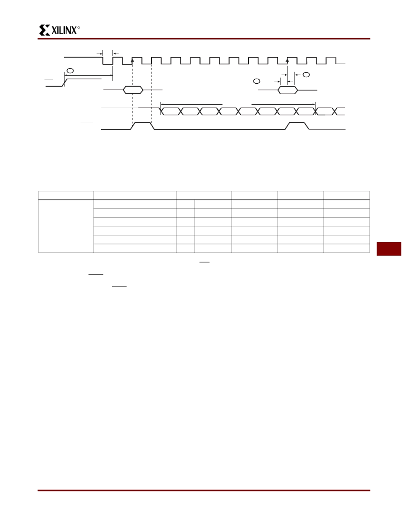
Notes:
1. Peripheral Synchronous mode can be considered Slave Parallel mode. An external CCLK provides timing, clocking in the
first
data byte on the
second
rising edge of CCLK after INIT goes high. Subsequent data bytes are clocked in on every
eighth consecutive rising edge of CCLK.
2. The RDY/BUSY line goes High for one CCLK period after data has been clocked in, although synchronous operation does
not require such a response.
3. The pin name RDY/BUSY is a misnomer. In synchronous peripheral mode this is really an ACKNOWLEDGE signal.
4.Note that data starts to shift out serially on the DOUT pin 0.5 CCLK periods after it was loaded in parallel. Therefore,
additional CCLK pulses are clearly required after the last byte has been loaded.
Figure 34: Synchronous Peripheral Mode Programming Switching Characteristics
0
DOUT
CCLK
1
2
3
4
5
6
7
BYTE
0
BYTE
1
BYTE 0 OUT
BYTE 1 OUT
RDY/BUSY
INIT
1
0
X6096
T
CCL
D0 - D7
T
IC
T
CD
T
DC
1
2
3
Description
Symbol
Min
5
60
0
50
60
Max
Units
μ
s
ns
ns
ns
ns
MHz
CCLK
INIT (High) setup time
D0 - D7 setup time
D0 - D7 hold time
CCLK High time
CCLK Low time
CCLK Frequency
1
2
3
T
IC
T
DC
T
CD
T
CCH
T
CCL
F
CC
8
相關(guān)PDF資料 |
PDF描述 |
|---|---|
| XC5202-6HQ208C | Field Programmable Gate Arrays |
| XC5202-6HQ240C | Field Programmable Gate Arrays |
| XC5202-6PG156C | Field Programmable Gate Arrays |
| XC5202-6PQ160C | Field Programmable Gate Arrays |
| XC68341CFT16 | Integrated Processor Users Manual |
相關(guān)代理商/技術(shù)參數(shù) |
參數(shù)描述 |
|---|---|
| XC5202-5PC84C | 制造商:Xilinx 功能描述: |
| XC5202-5PC84I | 制造商:未知廠家 制造商全稱:未知廠家 功能描述:Field Programmable Gate Array (FPGA) |
| XC5202-5PG156C | 制造商:XILINX 制造商全稱:XILINX 功能描述:Field Programmable Gate Arrays |
| XC5202-5PG156I | 制造商:未知廠家 制造商全稱:未知廠家 功能描述:Field Programmable Gate Array (FPGA) |
| XC5202-5PG191C | 制造商:XILINX 制造商全稱:XILINX 功能描述:Field Programmable Gate Arrays |
發(fā)布緊急采購,3分鐘左右您將得到回復(fù)。