- 您現(xiàn)在的位置:買賣IC網(wǎng) > PDF目錄374999 > XC4044XLA-08HQ240I (XILINX INC) XC4000XLA/XV Field Programmable Gate Arrays PDF資料下載
參數(shù)資料
| 型號: | XC4044XLA-08HQ240I |
| 廠商: | XILINX INC |
| 元件分類: | FPGA |
| 英文描述: | XC4000XLA/XV Field Programmable Gate Arrays |
| 中文描述: | FPGA, 1600 CLBS, 27000 GATES, 263 MHz, PQFP240 |
| 封裝: | QFP-240 |
| 文件頁數(shù): | 7/14頁 |
| 文件大小: | 142K |
| 代理商: | XC4044XLA-08HQ240I |
R
DS015 (v1.3) October 18, 1999 - Product Specification
6-163
XC4000XLA/XV Field Programmable Gate Arrays
6
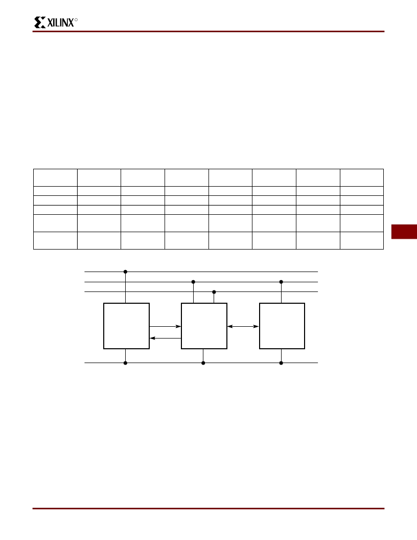
I/O Signalling Standards
XLA and XV devices are compatible with TTL, LVTTL, PCI
3V, PCI 5V and LVCMOS signalling. The various standards
are illustrated in
Table 6
and the signaling environment is
illustrated in
Figure 4
.
VCC Clamping
XLA/XV devices are fully 5V TTL I/O compatible if VCC
clamping is not enabled. The I/O pins can withstand input
voltages up to 7V. With VCC clamping enabled, the XLA/XV
devices will begin to clamp input voltages to one diode volt-
age drop above VCC. In both cases negative voltage is
clamped to one diode voltage drop below ground.
XLA/XV devices maintain LVTTL I/O compatibility when
VCC clamping is enabled, however full 5.0V TTL I/O com-
patibility is sacrificed.
Overshoot and Undershoot
Ringing wave forms are allowed on XLA/XV inputs as long
as undershoot is limited to -2.0V and overshoot is limited to
+7.0V and current is limited to 100 mA for less than 10 ns.
If VCC clamping is enabled then overshoot will begin to be
clamped at VCC/VCCIO plus one diode voltage drop and
undershoot will be clamped to ground minus one diode volt-
age drop. In either case the current must be limited to 100
mA per pin for less than 10 ns.
Express Configuration Mode
Express configuration mode is similar to Slave Serial con-
figuration mode, except that data is processed one byte per
CCLK cycle instead of one bit per CCLK cycle. An external
source is used to drive CCLK, while byte-wide data is
loaded directly into the configuration data shift registers
(
Figure 5
). A CCLK frequency of 10 MHz is equivalent to a
80 MHz serial rate, because eight bits of configuration data
are loaded per CCLK cycle. Express mode does not sup-
port CRC error checking, but does support constant-field
error checking. A length count is not used in Express mode.
Express mode must be specified as an option to the BitGen
program, which generates the bitstream. The Express
mode bitstream is not compatible with the other configura-
tion modes. Express mode is selected by a <010> on the
mode pins (M2, M1, M0).
The first byte of parallel configuration data must be avail-
able at the D inputs of the FPGA a short setup time before
the second rising CCLK edge. Subsequent data bytes are
Table 6: I/O Standards supported by XC4000XLA and XV FPGAs
Signaling
Standard
TTL
LVTTL
PCI5V
PCI3V
VCC
Clamping
Not allowed
OK
Not allowed
Required
Output Drive
12/24 mA
12/24 mA
24 mA
12 mA
V
IH_MAX
5.5
3.6
5.5
3.6
V
IH MIN
2.0
2.0
50% of
VCC/VCCIO
50% of
VCC/VCCIO
V
IL MAX
0.8
0.8
0.8
30% of
VCC/VCCIO
30% of
VCC/VCCIO
V
OH MIN
2.4
2.4
2.4
90% of
VCC/VCCIO
90% of
VCC/VCCIO
V
OL MAX
0.4
0.4
0.4
10% of
VCC/VCCIO
10% of
VCC/VCCIO
LVCMOS 3V
OK
12/24 mA
3.6
V
CC
(5 V)
5.0 V Power
3.3 V Power
2.5 V Power
Ground
TTL
LVTTL
5 Volt Device
V
CCIO
V
CCINT
LVTTL
XC4000XV
V
CC
(3.3 V)
3.3 Volt Device
X7147
Figure 4:
The Signalling Environment for XLA/XV FPGAS.
For XLA devices the VCCIO and VCCINT supplies are
replaced by a single 3.3 Volt VCC supply, however, all indicated I/O signalling is still supported.
相關(guān)PDF資料 |
PDF描述 |
|---|---|
| XC4044XL | XC4000E and XC4000X Series Field Programmable Gate Arrays |
| XC4044XLA | XC4000XLA/XV Field Programmable Gate Arrays |
| XC40250XV | XC4000XLA/XV Field Programmable Gate Arrays |
| XC40150XV | XC4000XLA/XV Field Programmable Gate Arrays |
| XC40110XV | XC4000XLA/XV Field Programmable Gate Arrays |
相關(guān)代理商/技術(shù)參數(shù) |
參數(shù)描述 |
|---|---|
| XC4044XLA09BG352C | 制造商:Xilinx 功能描述: |
| XC4044XLA-09BG352C | 制造商:Xilinx 功能描述: 制造商: 功能描述: 制造商:undefined 功能描述: |
| XC4044XLA-09BG352I | 制造商:Xilinx 功能描述: 制造商: 功能描述: 制造商:undefined 功能描述: |
| XC4044XLA-09BG432C | 制造商:Xilinx 功能描述: |
| XC4044XLA-09HQ160C | 制造商:Xilinx 功能描述: |
發(fā)布緊急采購,3分鐘左右您將得到回復(fù)。