- 您現(xiàn)在的位置:買賣IC網(wǎng) > PDF目錄374999 > XC4013E-5HG240C (Xilinx, Inc.) Programmable Gate Arrays PDF資料下載
參數(shù)資料
| 型號: | XC4013E-5HG240C |
| 廠商: | Xilinx, Inc. |
| 英文描述: | Programmable Gate Arrays |
| 中文描述: | 可編程門陣列 |
| 文件頁數(shù): | 39/68頁 |
| 文件大小: | 462K |
| 代理商: | XC4013E-5HG240C |
第1頁第2頁第3頁第4頁第5頁第6頁第7頁第8頁第9頁第10頁第11頁第12頁第13頁第14頁第15頁第16頁第17頁第18頁第19頁第20頁第21頁第22頁第23頁第24頁第25頁第26頁第27頁第28頁第29頁第30頁第31頁第32頁第33頁第34頁第35頁第36頁第37頁第38頁當前第39頁第40頁第41頁第42頁第43頁第44頁第45頁第46頁第47頁第48頁第49頁第50頁第51頁第52頁第53頁第54頁第55頁第56頁第57頁第58頁第59頁第60頁第61頁第62頁第63頁第64頁第65頁第66頁第67頁第68頁
R
May 14, 1999 (Version 1.6)
6-43
XC4000E and XC4000X Series Field Programmable Gate Arrays
6
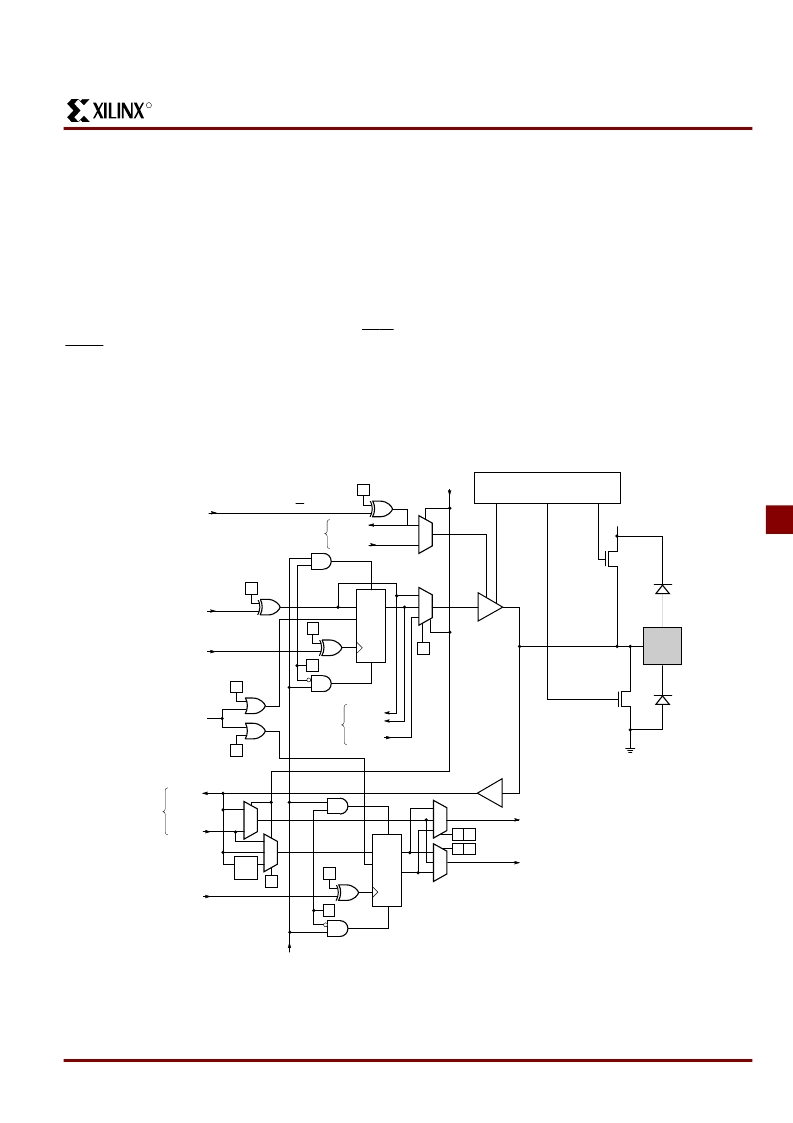
Figure 41 on page 44
is a diagram of the XC4000 Series
boundary scan logic. It includes three bits of Data Register
per IOB, the IEEE 1149.1 Test Access Port controller, and
the Instruction Register with decodes.
XC4000 Series devices can also be configured through the
boundary scan logic. See
“Readback” on page 55
.
Data Registers
The primary data register is the boundary scan register. For
each IOB pin in the FPGA, bonded or not, it includes three
bits for In, Out and 3-State Control. Non-IOB pins have
appropriate partial bit population for In or Out only. PRO-
GRAM, CCLK and DONE are not included in the boundary
scan register. Each EXTEST CAPTURE-DR state captures
all In, Out, and 3-state pins.
The data register also includes the following non-pin bits:
TDO.T, and TDO.O, which are always bits 0 and 1 of the
data register, respectively, and BSCANT.UPD, which is
always the last bit of the data register. These three bound-
ary scan bits are special-purpose Xilinx test signals.
The other standard data register is the single flip-flop
BYPASS register. It synchronizes data being passed
through the FPGA to the next downstream boundary scan
device.
The FPGA provides two additional data registers that can
be specified using the BSCAN macro. The FPGA provides
two user pins (BSCAN.SEL1 and BSCAN.SEL2) which are
the decodes of two user instructions. For these instructions,
two
corresponding
pins
BSCAN.TDO2) allow user scan data to be shifted out on
TDO. The data register clock (BSCAN.DRCK) is available
for control of test logic which the user may wish to imple-
ment with CLBs. The NAND of TCK and RUN-TEST-IDLE
is also provided (BSCAN.IDLE).
(BSCAN.TDO1
and
Figure 40: Block Diagram of XC4000E IOB with Boundary Scan (some details not shown).
XC4000X Boundary Scan Logic is Identical.
D
EC
Q
M
M
Q
L
rd
M
DELAY
M
M
M
M
Input Clock IK
I - capture
I - update
GLOBAL
S/R
FLIP-FLOP/LATCH
INVERT
S/R
Input Data 1 I1
Input Data 2 I2
X5792
PAD
V
CC
SLEW
RATE
PULL
UP
M
OUT
SEL
D
EC
Q
rd
M
M
M
INVERT
OUTPUT
M
M
INVERT
S/R
Ouput Clock OK
Clock Enable
Ouput Data O
O - update
Q - capture
O - capture
Boundary
Scan
M
EXTEST
TS - update
TS - capture
3-State TS
sd
sd
TS INV
OUTPUT
TS/OE
PULL
DOWN
INPUT
Boundary
Scan
Boundary
Scan
相關(guān)PDF資料 |
PDF描述 |
|---|---|
| XC4013E-5HG240I | Programmable Gate Arrays |
| XC4013E-5HG240M | Programmable Gate Arrays |
| XC4013E-6HG240C | Programmable Gate Arrays |
| XC4013E-6HG240I | Programmable Gate Arrays |
| XC4013E-6HG240M | Programmable Gate Arrays |
相關(guān)代理商/技術(shù)參數(shù) |
參數(shù)描述 |
|---|---|
| XC4013E-5HG240I | 制造商:XILINX 制造商全稱:XILINX 功能描述:Programmable Gate Arrays |
| XC4013E-5HG240M | 制造商:XILINX 制造商全稱:XILINX 功能描述:Programmable Gate Arrays |
| XC4013E-5HQ240C | 制造商:XILINX 制造商全稱:XILINX 功能描述:XC4000E and XC4000X Series Field Programmable Gate Arrays |
| XC4013E-5HQ240I | 制造商:XILINX 制造商全稱:XILINX 功能描述:XC4000E and XC4000X Series Field Programmable Gate Arrays |
| XC4013E-5HQ240M | 制造商:XILINX 制造商全稱:XILINX 功能描述:XC4000E and XC4000X Series Field Programmable Gate Arrays |
發(fā)布緊急采購,3分鐘左右您將得到回復(fù)。