- 您現(xiàn)在的位置:買賣IC網(wǎng) > PDF目錄374999 > XC4008 (Xilinx, Inc.) Logic Cell Array Family PDF資料下載
參數(shù)資料
| 型號(hào): | XC4008 |
| 廠商: | Xilinx, Inc. |
| 英文描述: | Logic Cell Array Family |
| 中文描述: | 邏輯單元陣列系列 |
| 文件頁(yè)數(shù): | 8/22頁(yè) |
| 文件大?。?/td> | 219K |
| 代理商: | XC4008 |
第1頁(yè)第2頁(yè)第3頁(yè)第4頁(yè)第5頁(yè)第6頁(yè)第7頁(yè)當(dāng)前第8頁(yè)第9頁(yè)第10頁(yè)第11頁(yè)第12頁(yè)第13頁(yè)第14頁(yè)第15頁(yè)第16頁(yè)第17頁(yè)第18頁(yè)第19頁(yè)第20頁(yè)第21頁(yè)第22頁(yè)
2-54
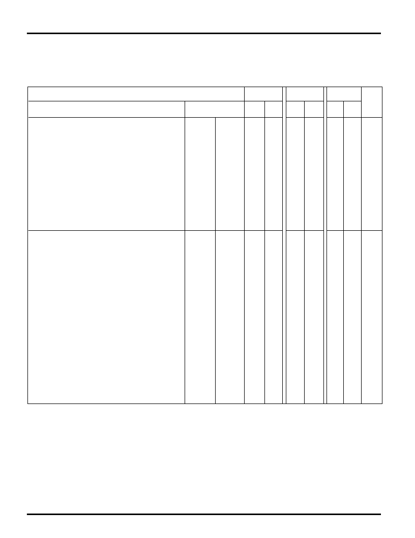
XC4000 Logic Cell Array Family
Write Operation
Address write cycle time
16 x 2
32 x 1
16 x 2
32 x 1
16 x 2
32 x 1
16 x 2
32 x 1
16 x 2
32 x 1
both
T
WC
T
WCT
T
WP
T
WPT
T
AS
T
AST
T
AH
T
AHT
T
DS
T
DST
T
DHT
9.0
9.0
5.0
5.0
2.0
2.0
2.0
2.0
4.0
5.0
2.0
8.0
8.0
4.0
4.0
2.0
2.0
2.0
2.0
4.0
5.0
2.0
8.0
8.0
4.0
4.0
2.0
2.0
2.0
2.0
4.0
5.0
2.0
ns
ns
ns
ns
ns
ns
ns
ns
ns
ns
ns
Write Enable pulse width (High)
Address set-up time before beginning of WE
Address hold time after end of WE
DIN set-up time before end of WE
DIN hold time after end of WE
Read Operation
Address read cycle time
16 x 2
32 x 1
16 x 2
32 x 1
T
RC
T
RCT
T
ILO
T
IHO
7.0
10.0
5.5
7.5
5.0
7.0
ns
ns
ns
ns
Data valid after address change
(no Write Enable)
6.0
8.0
4.5
7.0
4.0
6.0
Read Operation, Clocking Data into Flip-Flop
Address setup time before clock K
16 x 2
32 x 1
T
ICK
T
IHCK
6.0
8.0
4.5
6.0
4.5
6.0
ns
ns
Read During Write
Data valid after WE going active
(DIN stable before WE)
Data valid after DIN
(DIN change during WE)
16 x 2
32 x 1
16 x 2
32 x 1
T
WO
T
WOT
T
DO
T
DOT
12.0
15.0
11.0
14.0
10.0
12.0
9.0
11.0
9.0
11.0
8.5
11.0
ns
ns
ns
ns
Read During Write, Clocking Data into Flip-Flop
WE setup time before clock K
16 x 2
32 x 1
16 x 2
32 x 1
T
WCK
T
WCKT
T
DCK
T
DCKT
12.0
15.0
11.0
14.0
10.0
12.0
9.0
11.0
9.5
11.5
9.0
11.0
ns
ns
ns
ns
Data setup time before clock K
CLB Switching Characteristic Guidelines (continued)
Testing of the switching parameters is modeled after testing methods specified by MIL-M-38510/605. All devices are 100%
functionally tested. Since many internal timing parameters cannot be measured directly, they are derived from benchmark timing
patterns. The following guidelines reflect worst-case values over the recommended operating conditions. For more detailed, more
precise, and more up-to-date timing information, use the values provided by the XACT timing calculator and used in the simulator.
CLB RAM Option
Speed Grade
-6
-5
-4
Description
Symbol
Min
Max
Min Max
Min Max Units
Note: Timing for the 16 x 1 RAM option is identical to 16 x 2 RAM timing
相關(guān)PDF資料 |
PDF描述 |
|---|---|
| XC4028XLA | Field Programmable Gate Arrays(現(xiàn)場(chǎng)可編程門(mén)陣列) |
| XC4044XLA-08HQ240I | XC4000XLA/XV Field Programmable Gate Arrays |
| XC4044XL | XC4000E and XC4000X Series Field Programmable Gate Arrays |
| XC4044XLA | XC4000XLA/XV Field Programmable Gate Arrays |
| XC40250XV | XC4000XLA/XV Field Programmable Gate Arrays |
相關(guān)代理商/技術(shù)參數(shù) |
參數(shù)描述 |
|---|---|
| XC4008-4PQ160C | 制造商:未知廠家 制造商全稱:未知廠家 功能描述:Field Programmable Gate Array (FPGA) |
| XC4008-4PQ208C | 制造商:未知廠家 制造商全稱:未知廠家 功能描述:Field Programmable Gate Array (FPGA) |
| XC40085MQ208C | 制造商:XIL 功能描述:40085 XILINX'95 |
| XC4008-5MQ208C | 制造商:未知廠家 制造商全稱:未知廠家 功能描述:Field Programmable Gate Array (FPGA) |
| XC4008-5MQ208I | 制造商:未知廠家 制造商全稱:未知廠家 功能描述:Field Programmable Gate Array (FPGA) |
發(fā)布緊急采購(gòu),3分鐘左右您將得到回復(fù)。