- 您現(xiàn)在的位置:買賣IC網(wǎng) > PDF目錄374999 > XC4006 (Xilinx, Inc.) Logic Cell Array Family PDF資料下載
參數(shù)資料
| 型號(hào): | XC4006 |
| 廠商: | Xilinx, Inc. |
| 英文描述: | Logic Cell Array Family |
| 中文描述: | 邏輯單元陣列系列 |
| 文件頁數(shù): | 4/22頁 |
| 文件大?。?/td> | 219K |
| 代理商: | XC4006 |
2-50
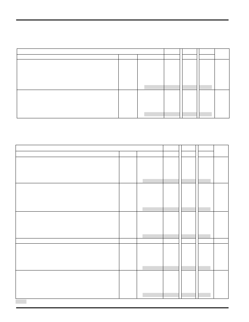
XC4000 Logic Cell Array Family
Speed Grade
-6
-5
-4
Description
Global Signal Distribution
From pad through
primary
buffer, to any clock K
Symbol
Device
Max
Max
Max
Units
T
PG
XC4003
XC4005
XC4006
XC4008
XC4010
XC4013
XC4025
XC4003
XC4005
XC4006
XC4008
XC4010
XC4013
XC4025
7.8
8.0
8.2
8.6
9.0
10.0
17.0
8.8
9.0
9.2
9.6
10.0
11.0
18.0
5.8
6.0
6.2
6.6
7.0
8.0
15.0
6.8
7.0
7.2
7.6
8.0
9.0
16.0
5.1
5.5
5.7
6.1
6.5
7.5
14.5
6.3
6.7
6.9
7.3
7.7
8.7
15.7
ns
ns
ns
ns
ns
ns
ns
ns
ns
ns
ns
ns
ns
ns
From pad through
secondary
buffer, to any clock K
T
SG
Speed Grade
Symbol
T
IO1
-6
-5
-4
Description
TBUF
driving a Horizontal Longline (L.L.)
I going High or Low to L.L. going High or Low,
while T is Low, i.e. buffer is constantly active
Device
XC4003
XC4005
XC4006
XC4008
XC4010
XC4013
XC4025
XC4003
XC4005
XC4006
XC4008
XC4010
XC4013
XC4025
XC4003
XC4005
XC4006
XC4008
XC4010
XC4013
XC4025
All devices
XC4003
XC4005
XC4006
XC4008
XC4010
XC4013
XC4025
XC4003
XC4005
XC4006
XC4008
XC4010
XC4013
XC4025
Max
8.8
10.0
10.6
11.1
11.7
13.0
20.0
9.3
10.5
11.1
11.6
12.2
13.5
23.5
10.7
12.0
12.6
13.2
13.8
15.1
23.0
3.0
24.0
26.0
28.0
30.0
32.0
36.0
52.0
11.6
12.0
13.0
14.0
15.0
17.0
24.0
Max
6.2
7.0
7.5
8.0
8.5
9.5
16.5
6.7
7.5
8.0
8.5
9.0
10.0
20.0
9.0
10.0
10.5
11.0
11.5
12.6
20.5
2.0
20.0
22.0
24.0
26.0
28.0
32.0
48.0
9.0
10.0
11.0
12.0
13.0
15.0
22.0
Max
4.4
5.5
6.0
6.5
7.0
7.5
14.5
5.0
6.0
6.5
7.0
7.5
8.0
18.0
7.2
8.0
8.5
9.0
9.5
11.1
19.0
1.8
14.0
16.0
18.0
20.0
22.0
26.0
42.0
7.0
8.0
9.0
10.0
11.0
13.0
20.0
Units
ns
ns
ns
ns
ns
ns
ns
ns
ns
ns
ns
ns
ns
ns
ns
ns
ns
ns
ns
ns
ns
ns
ns
ns
ns
ns
ns
ns
ns
ns
ns
ns
ns
ns
ns
ns
I going
Low to L.L. going from resistive pull-up
High to active Low, (TBUF configured as open drain)
T
IO2
T going Low to L.L. going from resistive pull-up or
floating High to active Low, (TBUF configured as
open drain or active buffer with I = Low)
T
ON
T going High
to TBUF going inactive, not driving L.L.
T going High to L.L. going from Low to High,
pulled up by a single resistor
T
OFF
T
PUS
T going High to L.L. going from Low to High,
pulled up by two resistors
T
PUF
Global Buffer Switching Characteristic Guidelines
Testing of the switching parameters is modeled after testing methods specified by MIL-M-38510/605. All devices are 100%
functionally tested. Since many internal timing parameters cannot be measured directly, they are derived from benchmark timing
patterns. The following guidelines reflect worst-case values over the recommended operating conditions. For more detailed, more
precise, and more up-to-date timing information, use the values provided by the XACT timing calculator and used in the simulator.
Horizontal Longline Switching Characteristic Guidelines
Testing of the switching parameters is modeled after testing methods specified by MIL-M-38510/605. All devices are 100%
functionally tested. Since many internal timing parameters cannot be measured directly, they are derived from benchmark timing
patterns. The following guidelines reflect worst-case values over the recommended operating conditions. For more detailed, more
precise, and more up-to-date timing information, use the values provided by the XACT timing calculator and used in the simulator.
PRELIMINARY
相關(guān)PDF資料 |
PDF描述 |
|---|---|
| XC4008 | Logic Cell Array Family |
| XC4028XLA | Field Programmable Gate Arrays(現(xiàn)場(chǎng)可編程門陣列) |
| XC4044XLA-08HQ240I | XC4000XLA/XV Field Programmable Gate Arrays |
| XC4044XL | XC4000E and XC4000X Series Field Programmable Gate Arrays |
| XC4044XLA | XC4000XLA/XV Field Programmable Gate Arrays |
相關(guān)代理商/技術(shù)參數(shù) |
參數(shù)描述 |
|---|---|
| XC4006-4PC84C | 制造商:未知廠家 制造商全稱:未知廠家 功能描述:Field Programmable Gate Array (FPGA) |
| XC4006-4PG156C | 制造商:Xilinx 功能描述: |
| XC4006-4PQ160C | 制造商:Xilinx 功能描述: |
| XC4006-4PQ208C | 制造商:未知廠家 制造商全稱:未知廠家 功能描述:Field Programmable Gate Array (FPGA) |
| XC4006-5PC84C | 制造商:Xilinx 功能描述: |
發(fā)布緊急采購,3分鐘左右您將得到回復(fù)。