- 您現(xiàn)在的位置:買賣IC網(wǎng) > PDF目錄374999 > XC4003H (Xilinx, Inc.) Logic Cell Array Families PDF資料下載
參數(shù)資料
| 型號(hào): | XC4003H |
| 廠商: | Xilinx, Inc. |
| 英文描述: | Logic Cell Array Families |
| 中文描述: | 家庭邏輯單元陣列 |
| 文件頁(yè)數(shù): | 2/22頁(yè) |
| 文件大?。?/td> | 219K |
| 代理商: | XC4003H |
第1頁(yè)當(dāng)前第2頁(yè)第3頁(yè)第4頁(yè)第5頁(yè)第6頁(yè)第7頁(yè)第8頁(yè)第9頁(yè)第10頁(yè)第11頁(yè)第12頁(yè)第13頁(yè)第14頁(yè)第15頁(yè)第16頁(yè)第17頁(yè)第18頁(yè)第19頁(yè)第20頁(yè)第21頁(yè)第22頁(yè)
2-48
XC4000 Logic Cell Array Family
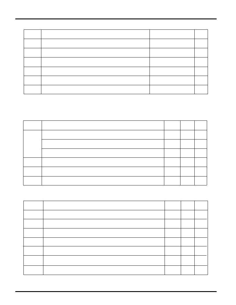
Absolute Maximum Ratings
Symbol
Description
Units
V
CC
Supply voltage relative to GND
–0.5 to +7.0
V
V
IN
Input voltage with respect to GND
–0.5 to V
CC
+0.5
V
V
TS
Voltage applied to 3-state output
–0.5 to V
CC
+0.5
V
T
STG
Storage temperature (ambient)
–65 to + 150
°
C
T
SOL
Maximum soldering temperature (10 s @ 1/16 in. = 1.5 mm)
+ 260
°
C
T
J
Junction temperature
+ 150
°
C
Note:
Stresses beyond those listed under Absolute Maximum Ratings may cause permanent damage to the device.
These are stress ratings only, and functional operation of the device at these or any other conditions beyond
those listed under Recommended Operating Conditions is not implied. Exposure to Absolute Maximum Ratings
conditions for extended periods of time may affect device reliability.
Operating Conditions
Symbol
Description
Min
Max
Units
V
CC
Supply voltage relative to GND Commercial 0
°
C to 85
°
C junction
4.75
5.25
V
Supply voltage relative to GND Industrial -40
°
C to 100
°
C junction
4.5
5.5
V
Supply voltage relative to GND
Military –55
°
C to 125
°
C case
4.5
5.5
V
V
IH
High-level input voltage (XC4000 has TTL-like input thresholds)
2.0
V
CC
V
V
IL
Low-level input voltage (XC4000 has TTL-like input thresholds)
0
0.8 V
T
IN
Input signal transition time
250
ns
DC Characteristics Over Operating Conditions
Symbol
Description
Min
Max
Units
V
OH
High-level output voltage @ I
OH
= –4.0 mA, V
CC
min
2.4
V
V
OL
Low-level output voltage @ I
OL
= 12.0 mA, V
CC
min (Note 1)
0.4
V
I
CCO
Quiescent LCA supply current (Note 2)
10
mA
I
IL
Leakage current
–10
+10
μ
A
C
IN
Input capacitance (sample tested)
15
pF
I
RIN
Pad pull-up (when selected) @ V
IN
= 0V (sample tested)
0.02
0.25
mA
I
RLL
Horizontal Long Line pull-up (when selected) @ logic Low
0.2
2.5
mA
Note: 1. With 50% of the outputs simultaneously sinking 12 mA.
2. With no output current loads, no active input or longline pull-up resistors, all package pins at V
CC
or GND, and
the LCA configured with a MakeBits tie option.
At junction temperatures above those listed as Operating Conditions, all delay parameters increase by 0.35% per
°
C.
相關(guān)PDF資料 |
PDF描述 |
|---|---|
| XC4006 | Logic Cell Array Family |
| XC4008 | Logic Cell Array Family |
| XC4028XLA | Field Programmable Gate Arrays(現(xiàn)場(chǎng)可編程門陣列) |
| XC4044XLA-08HQ240I | XC4000XLA/XV Field Programmable Gate Arrays |
| XC4044XL | XC4000E and XC4000X Series Field Programmable Gate Arrays |
相關(guān)代理商/技術(shù)參數(shù) |
參數(shù)描述 |
|---|---|
| XC4003H-4PG191C | 制造商:未知廠家 制造商全稱:未知廠家 功能描述:Field Programmable Gate Array (FPGA) |
| XC4003H-4PQ208C | 制造商:未知廠家 制造商全稱:未知廠家 功能描述:Field Programmable Gate Array (FPGA) |
| XC4003H-5PG191C | 制造商:未知廠家 制造商全稱:未知廠家 功能描述:Field Programmable Gate Array (FPGA) |
| XC4003H-5PQ208C | 制造商:未知廠家 制造商全稱:未知廠家 功能描述:Field Programmable Gate Array (FPGA) |
| XC4003H-6PG191C | 制造商:未知廠家 制造商全稱:未知廠家 功能描述:Field Programmable Gate Array (FPGA) |
發(fā)布緊急采購(gòu),3分鐘左右您將得到回復(fù)。