- 您現(xiàn)在的位置:買賣IC網(wǎng) > PDF目錄374982 > XC3142A-4VQ100I (XILINX INC) Field Programmable Gate Arrays (XC3000A/L, XC3100A/L) PDF資料下載
參數(shù)資料
| 型號: | XC3142A-4VQ100I |
| 廠商: | XILINX INC |
| 元件分類: | FPGA |
| 英文描述: | Field Programmable Gate Arrays (XC3000A/L, XC3100A/L) |
| 中文描述: | FPGA, 144 CLBS, 2000 GATES, 227 MHz, PQFP100 |
| 封裝: | PLASTIC, VQFP-100 |
| 文件頁數(shù): | 4/50頁 |
| 文件大小: | 474K |
| 代理商: | XC3142A-4VQ100I |
第1頁第2頁第3頁當(dāng)前第4頁第5頁第6頁第7頁第8頁第9頁第10頁第11頁第12頁第13頁第14頁第15頁第16頁第17頁第18頁第19頁第20頁第21頁第22頁第23頁第24頁第25頁第26頁第27頁第28頁第29頁第30頁第31頁第32頁第33頁第34頁第35頁第36頁第37頁第38頁第39頁第40頁第41頁第42頁第43頁第44頁第45頁第46頁第47頁第48頁第49頁第50頁
XC3000, XC3000A, XC3000L, XC3100, XC3100A Logic Cell Array Families
2-106
P9
P8
P7
P6
P5
P4
P3
P2
GND
PWR
DN
P11
P12
P13
U61
TCL
KIN
AD
AC
AB
AA
3-State Buffers With Access
to Horizontal Long Lines
Configurable Logic
Blocks
Interconnect Area
BB
BA
F
Configuration Memory
I/O Blocks
X3241
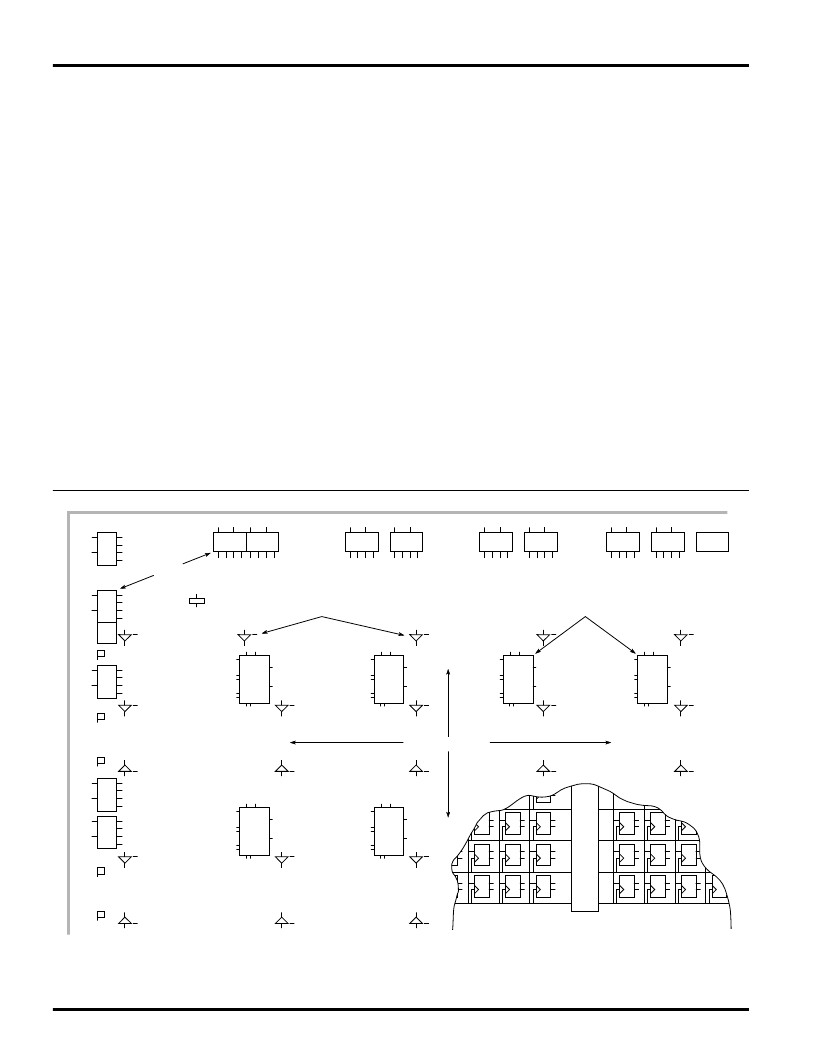
Figure 1.
Logic Cell Array Structure.
It consists of a perimeter of programmable I/O blocks, a core of configurable logic blocks and their interconnect resources.
These are all controlled by the distributed array of configuration program memory cells.
The XC3000 Logic Cell Array families provide a variety of
logic capacities, package styles, temperature ranges and
speed grades.
Architecture
The perimeter of configurable IOBs provides a pro-
grammable interface between the internal logic array and
the device package pins. The array of CLBs performs
user-specified logic functions. The interconnect resources
are programmed to form networks, carrying logic signals
among blocks, analogous to printed circuit board traces
connecting MSI/SSI packages.
The block logic functions are implemented by programmed
look-up tables. Functional options are implemented by
program-controlled multiplexers. Interconnecting networks
between blocks are implemented with metal segments
joined by program-controlled pass transistors.
These LCA functions are established by a configuration
program which is loaded into an internal, distributed array
of configuration memory cells. The configuration program
is loaded into the LCA device at power-up and may be
reloaded on command. The Logic Cell Array includes logic
and control signals to implement automatic or passive
configuration. Program data may be either bit serial or byte
parallel. The XACT development system generates the
configuration program bitstream used to configure the
LCA device. The memory loading process is independent
of the user logic functions.
Configuration Memory
The static memory cell used for the configuration memory
in the Logic Cell Array has been designed specifically for
high reliability and noise immunity. Integrity of the LCA
device configuration memory based on this design is
assured even under adverse conditions. Compared with
other programming alternatives, static memory provides
the best combination of high density, high performance,
high reliability and comprehensive testability. As shown in
Figure 2, the basic memory cell consists of two CMOS
inverters plus a pass transistor used for writing and read-
ing cell data. The cell is only written during configuration
and only read during readback. During normal operation,
the cell provides continuous control and the pass transistor
is off and does not affect cell stability. This is quite different
from the operation of conventional memory devices, in
which the cells are frequently read and rewritten.
相關(guān)PDF資料 |
PDF描述 |
|---|---|
| XC3142A-2PC84C | Field Programmable Gate Arrays (XC3000A/L, XC3100A/L) |
| XC3142A-2PC84I | ECONOLINE: RSZ/P - 1kVDC |
| XC3142A-3PC84C | Field Programmable Gate Arrays (XC3000A/L, XC3100A/L) |
| XC3142A-3PC84I | RSZ Series - Econoline Regulated DC-DC Converters; Input Voltage (Vdc): 05V; Output Voltage (Vdc): 05V; Power: 1W; 1kVDC & 2kVDC Isolation; UL94V-0 Package Material; No Heatsink Required; No External Components Required; Toroidal Magnetics; Optional Continuous Short Circuit Protected |
| XC3142A-3PQ100I | Field Programmable Gate Arrays (XC3000A/L, XC3100A/L) |
相關(guān)代理商/技術(shù)參數(shù) |
參數(shù)描述 |
|---|---|
| XC3142A-5CB100B | 制造商:未知廠家 制造商全稱:未知廠家 功能描述:Field Programmable Gate Array (FPGA) |
| XC3142A-5CB100M | 制造商:未知廠家 制造商全稱:未知廠家 功能描述:Field Programmable Gate Array (FPGA) |
| XC3142A5PC84C | 制造商:XILINX 功能描述:* |
| XC3142A-5PG132B | 制造商:未知廠家 制造商全稱:未知廠家 功能描述:Field Programmable Gate Array (FPGA) |
| XC3142A-5PG132M | 制造商:未知廠家 制造商全稱:未知廠家 功能描述:Field Programmable Gate Array (FPGA) |
發(fā)布緊急采購,3分鐘左右您將得到回復(fù)。