- 您現(xiàn)在的位置:買賣IC網(wǎng) > PDF目錄374983 > XC3042A-7TQ144C (XILINX INC) Field Programmable Gate Arrays (XC3000A/L, XC3100A/L) PDF資料下載
參數(shù)資料
| 型號: | XC3042A-7TQ144C |
| 廠商: | XILINX INC |
| 元件分類: | FPGA |
| 英文描述: | Field Programmable Gate Arrays (XC3000A/L, XC3100A/L) |
| 中文描述: | FPGA, 144 CLBS, 2000 GATES, 113 MHz, PQFP144 |
| 封裝: | PLASTIC, TQFP-144 |
| 文件頁數(shù): | 24/50頁 |
| 文件大小: | 474K |
| 代理商: | XC3042A-7TQ144C |
第1頁第2頁第3頁第4頁第5頁第6頁第7頁第8頁第9頁第10頁第11頁第12頁第13頁第14頁第15頁第16頁第17頁第18頁第19頁第20頁第21頁第22頁第23頁當(dāng)前第24頁第25頁第26頁第27頁第28頁第29頁第30頁第31頁第32頁第33頁第34頁第35頁第36頁第37頁第38頁第39頁第40頁第41頁第42頁第43頁第44頁第45頁第46頁第47頁第48頁第49頁第50頁
XC3000, XC3000A, XC3000L, XC3100, XC3100A Logic Cell Array Families
2-126
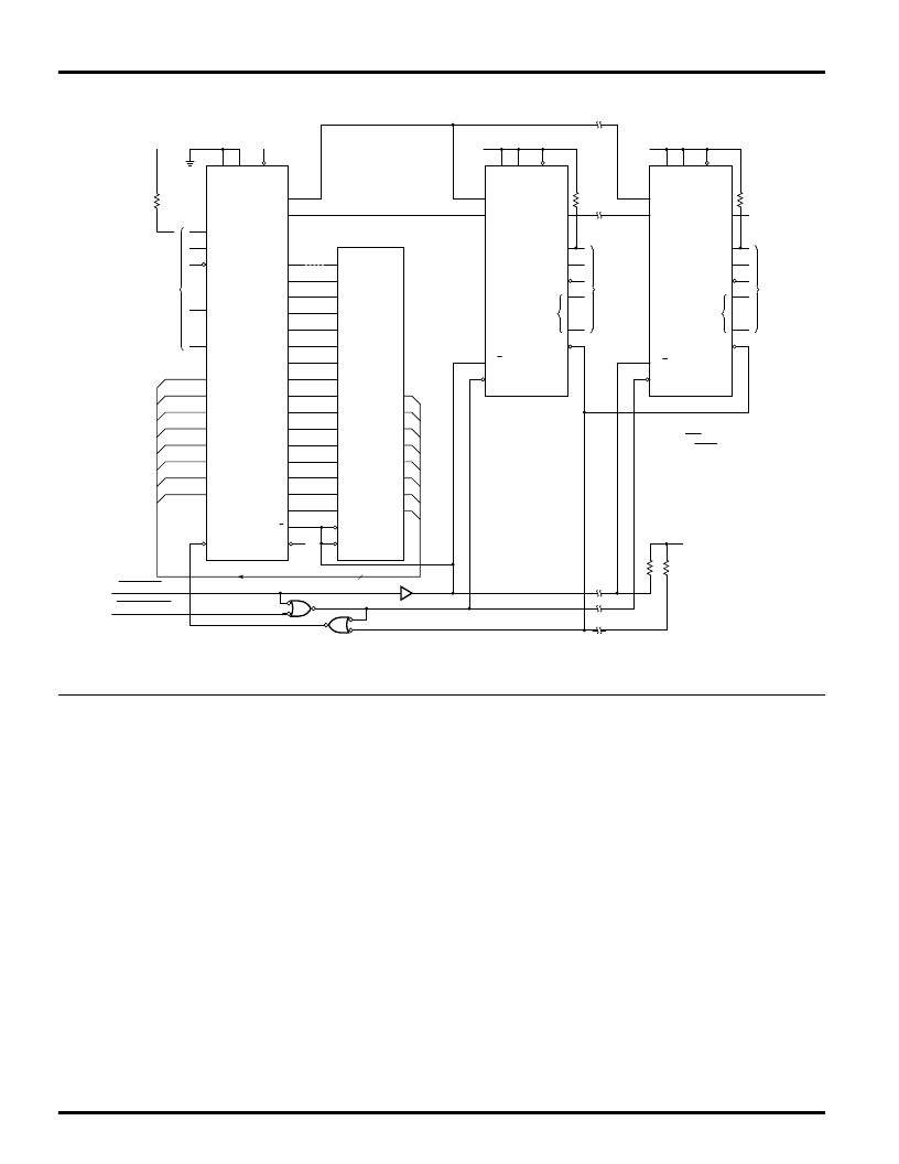
Master Parallel Mode
Figure 22.
Master Parallel Mode
X3159
RCLK
General-
Purpose
User I/O
Pins
M0 M1PWRDWN
M2
HDC
Other
I/O Pins
D7
D6
D5
D4
D3
D2
D1
D0
A15
A14
A13
A12
A11
A10
A9
A8
A7
A6
A5
A4
A3
A2
A1
A0
A10
A9
A8
A7
A6
A5
A4
A3
A2
A1
A0
D7
D6
D5
D4
D3
D2
D1
D0
+5 V
.
CE
OE
LCA
Master
CCLK
DOUT
System Reset
A11
A12
A13
A14
A15
EPROM
RESET
.
Other
I/O Pins
DOUT
M2
HDC
LDC
LCA
Slave #1
+5 V
M0 M1PWRDWN
CCLK
DIN
D/P
Reset
DOUT
LCA
Slave #n
+5 V
M0 M1PWRDWN
CCLK
DIN
D/P
General-
Purpose
User I/O
Pins
RESET
...
+5 V
8
INIT
.
M2
HDC
LDC
INIT
General-
Purpose
User I/O
Pins
+5 V
D/P
Other
I/O Pins
Note: XC2000 Devices Do Not
Have INIT to Hold Off a Master
Device. Reset of a Master Device
Should be Asserted by an External
Timing Circuit to Allow for LCA CCLK
Variations in Clear State Time.
Open
Collector
INITN.C.
Reprogram
5 k‰
5 k‰
5 k‰
5 k‰ Each
If Readback is
Activated, a
5-k‰ Resistor is
Required in
Series With M1
*
*
*
*
internal delay of 1.5 CCLK periods, after the rising CCLK
edge that accepts a byte of data, and also changes the
EPROM address, until the falling CCLK edge that makes
the LSB (D0) of this byte appear at DOUT. This means that
DOUT changes on the falling CCLK edge, and the next
LCA device in the daisy chain accepts data on the subse-
quent rising CCLK edge.
In Master Parallel mode, the lead LCA device directly
addresses an industry-standard byte-wide EPROM and
accepts eight data bits right before incrementing (or
decrementing) the address outputs.
The eight data bits are serialized in the lead LCA device,
which then presents the preamble data (and all data that
overflows the lead device) on the DOUT pin. There is an
相關(guān)PDF資料 |
PDF描述 |
|---|---|
| XC3042A-7TQ144I | Field Programmable Gate Arrays (XC3000A/L, XC3100A/L) |
| XC3164A-3PC84I | Field Programmable Gate Arrays (XC3000A/L, XC3100A/L) |
| XC3164A-3PQ160C | Field Programmable Gate Arrays (XC3000A/L, XC3100A/L) |
| XC3164A-3PQ160I | Field Programmable Gate Arrays (XC3000A/L, XC3100A/L) |
| XC3164A-3TQ144C | Field Programmable Gate Arrays (XC3000A/L, XC3100A/L) |
相關(guān)代理商/技術(shù)參數(shù) |
參數(shù)描述 |
|---|---|
| XC3042A-7TQ144I | 制造商:XILINX 制造商全稱:XILINX 功能描述:Field Programmable Gate Arrays (XC3000A/L, XC3100A/L) |
| XC3042A-7VQ100C | 功能描述:IC FIELD PROG GATE ARRAY 100 PIN RoHS:否 類別:集成電路 (IC) >> 嵌入式 - FPGA(現(xiàn)場可編程門陣列) 系列:XC3000A/L 產(chǎn)品變化通告:XC4000(E,L) Discontinuation 01/April/2002 標(biāo)準(zhǔn)包裝:24 系列:XC4000E/X LAB/CLB數(shù):100 邏輯元件/單元數(shù):238 RAM 位總計:3200 輸入/輸出數(shù):80 門數(shù):3000 電源電壓:4.5 V ~ 5.5 V 安裝類型:表面貼裝 工作溫度:-40°C ~ 100°C 封裝/外殼:120-BCBGA 供應(yīng)商設(shè)備封裝:120-CPGA(34.55x34.55) |
| XC3042A-7VQ100I | 制造商:Xilinx 功能描述: |
| XC3042B | 制造商:未知廠家 制造商全稱:未知廠家 功能描述: |
| XC3042L | 制造商:XILINX 制造商全稱:XILINX 功能描述:Field Programmable Gate Arrays |
發(fā)布緊急采購,3分鐘左右您將得到回復(fù)。