- 您現(xiàn)在的位置:買賣IC網(wǎng) > PDF目錄374983 > XC3042A-7TQ144C (XILINX INC) Field Programmable Gate Arrays (XC3000A/L, XC3100A/L) PDF資料下載
參數(shù)資料
| 型號(hào): | XC3042A-7TQ144C |
| 廠商: | XILINX INC |
| 元件分類: | FPGA |
| 英文描述: | Field Programmable Gate Arrays (XC3000A/L, XC3100A/L) |
| 中文描述: | FPGA, 144 CLBS, 2000 GATES, 113 MHz, PQFP144 |
| 封裝: | PLASTIC, TQFP-144 |
| 文件頁(yè)數(shù): | 19/50頁(yè) |
| 文件大小: | 474K |
| 代理商: | XC3042A-7TQ144C |
第1頁(yè)第2頁(yè)第3頁(yè)第4頁(yè)第5頁(yè)第6頁(yè)第7頁(yè)第8頁(yè)第9頁(yè)第10頁(yè)第11頁(yè)第12頁(yè)第13頁(yè)第14頁(yè)第15頁(yè)第16頁(yè)第17頁(yè)第18頁(yè)當(dāng)前第19頁(yè)第20頁(yè)第21頁(yè)第22頁(yè)第23頁(yè)第24頁(yè)第25頁(yè)第26頁(yè)第27頁(yè)第28頁(yè)第29頁(yè)第30頁(yè)第31頁(yè)第32頁(yè)第33頁(yè)第34頁(yè)第35頁(yè)第36頁(yè)第37頁(yè)第38頁(yè)第39頁(yè)第40頁(yè)第41頁(yè)第42頁(yè)第43頁(yè)第44頁(yè)第45頁(yè)第46頁(yè)第47頁(yè)第48頁(yè)第49頁(yè)第50頁(yè)
2-121
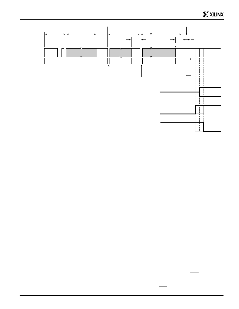
Preamble
Length Count
Data
12
24
4
Data Frame
Start
Bit
Start
Bit
3
4
Last Frame
Postamble
I/O Active
DONE
Internal Reset
Length Count*
The configuration data consists of a composite
40-bit preamble/length count, followed by one or
more concatenated LCA programs, separated by
4-bit postambles. An additional final postamble bit
is added for each slave device and the result rounded
up to a byte boundary. The length count is two less
than the number of resulting bits.
Timing of the assertion of DONE and
termination of the INTERNAL RESET
may each be programmed to occur
one cycle before or after the I/O outputs
become active.
Heavy lines indicate the default condition
X5303
PROGRAM
Weak Pull-Up
*
Stop
3
STOP
DIN
Figure 20.
Configuration and Start-up of One or More LCA Devices.
storage at power-up and after a re-program signal. Several
methods of automatic and controlled loading of the re-
quired data are available. Logic levels applied to mode
selection pins at the start of configuration time determine
the method to be used. See Table 1. The data may be
either bit-serial or byte-parallel, depending on the configu-
ration mode. The different LCA devices have different
sizes and numbers of data frames. To maintain compatibil-
ity between various device types, the Xilinx product fami-
lies use compatible configuration formats. For the
XC3020, configuration requires 14779 bits for each de-
vice, arranged in 197 data frames. An additional 40 bits are
used in the header. See Figure 20. The specific data
format for each device is produced by the MakeBits
command of the development system and one or more of
these files can then be combined and appended to a length
count preamble and be transformed into a PROM format
file by the MakePROM command of the XACT develop-
ment system. A compatibility exception precludes the use
of an XC2000-series device as the master for XC3000-
series devices if their DONE or RESET are programmed
to occur after their outputs become active.
The Tie Option of the MakeBits program defines output
levels of unused blocks of a design and connects these to
unused routing resources. This prevents indeterminate
levels that might produce parasitic supply currents. If
unused blocks are not sufficient to complete the tie, the
Flagnet command of EDITLCA can be used to indicate
nets which must not be used to drive the remaining unused
routing, as that might affect timing of user nets. Norestore
will retain the results of tie for timing analysis with Querynet
before Restore returns the design to the untied condition.
Tie can be omitted for quick breadboard iterations where
a few additional milliamps of I
CC
are acceptable.
The configuration bitstream begins with eight High pre-
amble bits, a 4-bit preamble code and a 24-bit length count.
When configuration is initiated, a counter in the LCA device
is set to zero and begins to count the total number of
configuration clock cycles applied to the device. As each
configuration data frame is supplied to the LCA device, it is
internally assembled into a data word, which is then loaded
in parallel into one word of the internal configuration
memory array. The configuration loading process is com-
plete when the current length count equals the loaded
length count and the required configuration program data
frames have been written. Internal user flip-flops are held
Reset during configuration.
Two user-programmable pins are defined in the unconfig-
ured Logic Cell array. High During Configuration (HDC)
and Low During Configuration (LDC) as well as
DONE/PROG may be used as external control signals
during configuration. In Master mode configurations it is
convenient to use LDC as an active-Low EPROM Chip
相關(guān)PDF資料 |
PDF描述 |
|---|---|
| XC3042A-7TQ144I | Field Programmable Gate Arrays (XC3000A/L, XC3100A/L) |
| XC3164A-3PC84I | Field Programmable Gate Arrays (XC3000A/L, XC3100A/L) |
| XC3164A-3PQ160C | Field Programmable Gate Arrays (XC3000A/L, XC3100A/L) |
| XC3164A-3PQ160I | Field Programmable Gate Arrays (XC3000A/L, XC3100A/L) |
| XC3164A-3TQ144C | Field Programmable Gate Arrays (XC3000A/L, XC3100A/L) |
相關(guān)代理商/技術(shù)參數(shù) |
參數(shù)描述 |
|---|---|
| XC3042A-7TQ144I | 制造商:XILINX 制造商全稱:XILINX 功能描述:Field Programmable Gate Arrays (XC3000A/L, XC3100A/L) |
| XC3042A-7VQ100C | 功能描述:IC FIELD PROG GATE ARRAY 100 PIN RoHS:否 類別:集成電路 (IC) >> 嵌入式 - FPGA(現(xiàn)場(chǎng)可編程門陣列) 系列:XC3000A/L 產(chǎn)品變化通告:XC4000(E,L) Discontinuation 01/April/2002 標(biāo)準(zhǔn)包裝:24 系列:XC4000E/X LAB/CLB數(shù):100 邏輯元件/單元數(shù):238 RAM 位總計(jì):3200 輸入/輸出數(shù):80 門數(shù):3000 電源電壓:4.5 V ~ 5.5 V 安裝類型:表面貼裝 工作溫度:-40°C ~ 100°C 封裝/外殼:120-BCBGA 供應(yīng)商設(shè)備封裝:120-CPGA(34.55x34.55) |
| XC3042A-7VQ100I | 制造商:Xilinx 功能描述: |
| XC3042B | 制造商:未知廠家 制造商全稱:未知廠家 功能描述: |
| XC3042L | 制造商:XILINX 制造商全稱:XILINX 功能描述:Field Programmable Gate Arrays |
發(fā)布緊急采購(gòu),3分鐘左右您將得到回復(fù)。