- 您現(xiàn)在的位置:買賣IC網(wǎng) > PDF目錄374970 > XC2V8000 (Xilinx, Inc.) Virtex-II Platform FPGAs: Complete Data Sheet PDF資料下載
參數(shù)資料
| 型號: | XC2V8000 |
| 廠商: | Xilinx, Inc. |
| 元件分類: | FPGA |
| 英文描述: | Virtex-II Platform FPGAs: Complete Data Sheet |
| 中文描述: | 的Virtex - II FPGA平臺:完整的數(shù)據(jù)手冊 |
| 文件頁數(shù): | 82/311頁 |
| 文件大?。?/td> | 1836K |
| 代理商: | XC2V8000 |
第1頁第2頁第3頁第4頁第5頁第6頁第7頁第8頁第9頁第10頁第11頁第12頁第13頁第14頁第15頁第16頁第17頁第18頁第19頁第20頁第21頁第22頁第23頁第24頁第25頁第26頁第27頁第28頁第29頁第30頁第31頁第32頁第33頁第34頁第35頁第36頁第37頁第38頁第39頁第40頁第41頁第42頁第43頁第44頁第45頁第46頁第47頁第48頁第49頁第50頁第51頁第52頁第53頁第54頁第55頁第56頁第57頁第58頁第59頁第60頁第61頁第62頁第63頁第64頁第65頁第66頁第67頁第68頁第69頁第70頁第71頁第72頁第73頁第74頁第75頁第76頁第77頁第78頁第79頁第80頁第81頁當(dāng)前第82頁第83頁第84頁第85頁第86頁第87頁第88頁第89頁第90頁第91頁第92頁第93頁第94頁第95頁第96頁第97頁第98頁第99頁第100頁第101頁第102頁第103頁第104頁第105頁第106頁第107頁第108頁第109頁第110頁第111頁第112頁第113頁第114頁第115頁第116頁第117頁第118頁第119頁第120頁第121頁第122頁第123頁第124頁第125頁第126頁第127頁第128頁第129頁第130頁第131頁第132頁第133頁第134頁第135頁第136頁第137頁第138頁第139頁第140頁第141頁第142頁第143頁第144頁第145頁第146頁第147頁第148頁第149頁第150頁第151頁第152頁第153頁第154頁第155頁第156頁第157頁第158頁第159頁第160頁第161頁第162頁第163頁第164頁第165頁第166頁第167頁第168頁第169頁第170頁第171頁第172頁第173頁第174頁第175頁第176頁第177頁第178頁第179頁第180頁第181頁第182頁第183頁第184頁第185頁第186頁第187頁第188頁第189頁第190頁第191頁第192頁第193頁第194頁第195頁第196頁第197頁第198頁第199頁第200頁第201頁第202頁第203頁第204頁第205頁第206頁第207頁第208頁第209頁第210頁第211頁第212頁第213頁第214頁第215頁第216頁第217頁第218頁第219頁第220頁第221頁第222頁第223頁第224頁第225頁第226頁第227頁第228頁第229頁第230頁第231頁第232頁第233頁第234頁第235頁第236頁第237頁第238頁第239頁第240頁第241頁第242頁第243頁第244頁第245頁第246頁第247頁第248頁第249頁第250頁第251頁第252頁第253頁第254頁第255頁第256頁第257頁第258頁第259頁第260頁第261頁第262頁第263頁第264頁第265頁第266頁第267頁第268頁第269頁第270頁第271頁第272頁第273頁第274頁第275頁第276頁第277頁第278頁第279頁第280頁第281頁第282頁第283頁第284頁第285頁第286頁第287頁第288頁第289頁第290頁第291頁第292頁第293頁第294頁第295頁第296頁第297頁第298頁第299頁第300頁第301頁第302頁第303頁第304頁第305頁第306頁第307頁第308頁第309頁第310頁第311頁
Virtex-II Platform FPGAs: DC and Switching Characteristics
R
DS031-3 (v3.0) August 1, 2003
Product Specification
1-800-255-7778Module 3 of 4
34
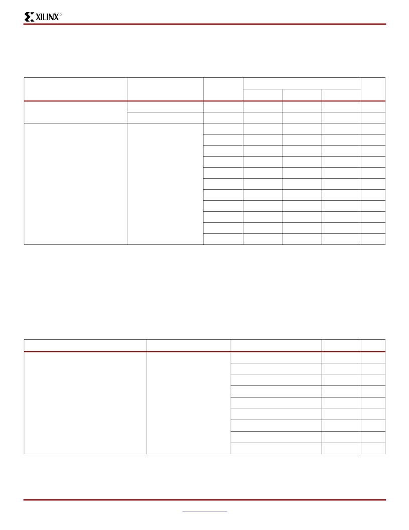
Source-Synchronous Switching Characteristics
The parameters in this section provide the necessary values for calculating timing budgets for Virtex-II source-synchronous
transmitter and receiver data-valid windows.
Table 41:
Duty Cycle Distortion and Clock-Tree Skew
Description
Symbol
Device
Speed Grade
Units
–
6
–
5
–
4
Duty Cycle Distortion
(1)
T
DCD_CLK0
T
DCD_CLK180
All
140
140
140
ps
All
50
50
50
ps
Clock Tree Skew
(2)
T
CKSKEW
XC2V40
TBD
50
TBD
ps
XC2V80
TBD
50
TBD
ps
XC2V250
TBD
50
TBD
ps
XC2V500
TBD
50
TBD
ps
XC2V1000
TBD
80
TBD
ps
XC2V1500
TBD
80
TBD
ps
XC2V2000
TBD
100
TBD
ps
XC2V3000
TBD
100
TBD
ps
XC2V4000
TBD
TBD
TBD
ps
XC2V6000
TBD
500
TBD
ps
XC2V8000
TBD
TBD
TBD
ps
Notes:
1.
These parameters represent the worst-case duty cycle distortion observable at the pins of the device using LVDS output buffers. For
cases where other I/O standards are used, IBIS can be used to calculate any additional duty cycle distortion that might be caused
by asymmetrical rise/fall times.
T
DCD_CLK0
applies to cases where local (IOB) inversion is used to provide the negative-edge clock to the DDR element in the I/O.
T
DCD_CLK180
applies to cases where the CLK180 output of the DCM is used to provide the negative-edge clock to the DDR element
in the I/O.
This value represents the worst-case clock-tree skew observable between sequential I/O elements. Significantly less clock-tree skew
exists for I/O registers that are close to each other and fed by the same or adjacent clock-tree branches. Use the Xilinx FPGA_Editor
and Timing Analyzer tools to evaluate clock skew specific to your application.
2.
Table 42:
Package Skew
Description
Symbol
Device/Package
Value
Units
Package Skew
(1)
T
PKGSKEW
XC2V1000 / FF896
130
ps
XC2V3000 / FF1152
115
ps
XC2V3000 / BF957
130
ps
XC2V4000 / FF1152
130
ps
XC2V4000 / FF1517
200
ps
XC2V4000 / BF957
140
ps
XC2V6000 / FF1152
90
ps
XC2V6000 / FF1517
105
ps
XC2V6000 / BF957
105
ps
Notes:
1.
These values represent the worst-case skew between any two balls of the package: shortest flight time to longest flight time from Pad
to Ball (7.1ps per mm).
Package trace length information is available for these device/package combinations. This information can be used to deskew the
package.
2.
相關(guān)PDF資料 |
PDF描述 |
|---|---|
| XC2V80-4BF957C | Virtex-II 1.5V Field-Programmable Gate Arrays |
| XC2V80-4BF957I | Virtex-II 1.5V Field-Programmable Gate Arrays |
| XC2V80-4BG575C | Virtex-II 1.5V Field-Programmable Gate Arrays |
| XC2V80-4BG575I | Virtex-II 1.5V Field-Programmable Gate Arrays |
| XC2V80-4BG728C | Virtex-II 1.5V Field-Programmable Gate Arrays |
相關(guān)代理商/技術(shù)參數(shù) |
參數(shù)描述 |
|---|---|
| XC2V8000-4BF957C | 制造商:XILINX 制造商全稱:XILINX 功能描述:Virtex-II 1.5V Field-Programmable Gate Arrays |
| XC2V8000-4BF957I | 制造商:XILINX 制造商全稱:XILINX 功能描述:Virtex-II 1.5V Field-Programmable Gate Arrays |
| XC2V8000-4CS144C | 制造商:XILINX 制造商全稱:XILINX 功能描述:Virtex-II Platform FPGAs: Complete Data Sheet |
| XC2V8000-4CS144I | 制造商:XILINX 制造商全稱:XILINX 功能描述:Virtex-II Platform FPGAs: Complete Data Sheet |
| XC2V8000-4FF1152C | 制造商:XILINX 制造商全稱:XILINX 功能描述:Virtex-II 1.5V Field-Programmable Gate Arrays |
發(fā)布緊急采購,3分鐘左右您將得到回復(fù)。