- 您現(xiàn)在的位置:買賣IC網(wǎng) > PDF目錄374970 > XC2V80-4BF957I (Xilinx, Inc.) Virtex-II 1.5V Field-Programmable Gate Arrays PDF資料下載
參數(shù)資料
| 型號: | XC2V80-4BF957I |
| 廠商: | Xilinx, Inc. |
| 英文描述: | Virtex-II 1.5V Field-Programmable Gate Arrays |
| 中文描述: | 的Virtex - II 1.5V的現(xiàn)場可編程門陣列 |
| 文件頁數(shù): | 11/311頁 |
| 文件大小: | 1836K |
| 代理商: | XC2V80-4BF957I |
第1頁第2頁第3頁第4頁第5頁第6頁第7頁第8頁第9頁第10頁當(dāng)前第11頁第12頁第13頁第14頁第15頁第16頁第17頁第18頁第19頁第20頁第21頁第22頁第23頁第24頁第25頁第26頁第27頁第28頁第29頁第30頁第31頁第32頁第33頁第34頁第35頁第36頁第37頁第38頁第39頁第40頁第41頁第42頁第43頁第44頁第45頁第46頁第47頁第48頁第49頁第50頁第51頁第52頁第53頁第54頁第55頁第56頁第57頁第58頁第59頁第60頁第61頁第62頁第63頁第64頁第65頁第66頁第67頁第68頁第69頁第70頁第71頁第72頁第73頁第74頁第75頁第76頁第77頁第78頁第79頁第80頁第81頁第82頁第83頁第84頁第85頁第86頁第87頁第88頁第89頁第90頁第91頁第92頁第93頁第94頁第95頁第96頁第97頁第98頁第99頁第100頁第101頁第102頁第103頁第104頁第105頁第106頁第107頁第108頁第109頁第110頁第111頁第112頁第113頁第114頁第115頁第116頁第117頁第118頁第119頁第120頁第121頁第122頁第123頁第124頁第125頁第126頁第127頁第128頁第129頁第130頁第131頁第132頁第133頁第134頁第135頁第136頁第137頁第138頁第139頁第140頁第141頁第142頁第143頁第144頁第145頁第146頁第147頁第148頁第149頁第150頁第151頁第152頁第153頁第154頁第155頁第156頁第157頁第158頁第159頁第160頁第161頁第162頁第163頁第164頁第165頁第166頁第167頁第168頁第169頁第170頁第171頁第172頁第173頁第174頁第175頁第176頁第177頁第178頁第179頁第180頁第181頁第182頁第183頁第184頁第185頁第186頁第187頁第188頁第189頁第190頁第191頁第192頁第193頁第194頁第195頁第196頁第197頁第198頁第199頁第200頁第201頁第202頁第203頁第204頁第205頁第206頁第207頁第208頁第209頁第210頁第211頁第212頁第213頁第214頁第215頁第216頁第217頁第218頁第219頁第220頁第221頁第222頁第223頁第224頁第225頁第226頁第227頁第228頁第229頁第230頁第231頁第232頁第233頁第234頁第235頁第236頁第237頁第238頁第239頁第240頁第241頁第242頁第243頁第244頁第245頁第246頁第247頁第248頁第249頁第250頁第251頁第252頁第253頁第254頁第255頁第256頁第257頁第258頁第259頁第260頁第261頁第262頁第263頁第264頁第265頁第266頁第267頁第268頁第269頁第270頁第271頁第272頁第273頁第274頁第275頁第276頁第277頁第278頁第279頁第280頁第281頁第282頁第283頁第284頁第285頁第286頁第287頁第288頁第289頁第290頁第291頁第292頁第293頁第294頁第295頁第296頁第297頁第298頁第299頁第300頁第301頁第302頁第303頁第304頁第305頁第306頁第307頁第308頁第309頁第310頁第311頁
Virtex-II Platform FPGAs: Detailed Description
R
DS031-2 (v3.0) August 1, 2003
Product Specification
1-800-255-7778Module 2 of 4
3
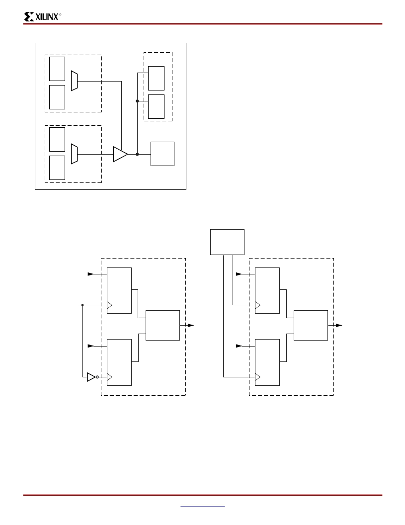
The DDR mechanism shown in
Figure 3
can be used to mir-
ror a copy of the clock on the output. This is useful for prop-
agating a clock along the data that has an identical delay. It
is also useful for multiple clock generation, where there is a
unique clock driver for every clock load. Virtex-II devices
can produce many copies of a clock with very little skew.
Each group of two registers has a clock enable signal (ICE
for the input registers, OCE for the output registers, and
TCE for the 3-state registers). The clock enable signals are
active High by default. If left unconnected, the clock enable
for that storage element defaults to the active state.
Each IOB block has common synchronous or asynchronous
set and reset (SR and REV signals).
SR forces the storage element into the state specified by the
SRHIGH or SRLOW attribute. SRHIGH forces a logic “1”.
SRLOW forces a logic “0”. When SR is used, a second input
(REV) forces the storage element into the opposite state. The
reset condition predominates over the set condition. The ini-
tial state after configuration or global initialization state is
defined by a separate INIT0 and INIT1 attribute. By default,
the SRLOW attribute forces INIT0, and the SRHIGH attribute
forces INIT1.
For each storage element, the SRHIGH, SRLOW, INIT0,
and INIT1 attributes are independent. Synchronous or
asynchronous set / reset is consistent in an IOB block.
All the control signals have independent polarity. Any
inverter placed on a control input is automatically absorbed.
Each register or latch (independent of all other registers or
latches) (see
Figure 4
) can be configured as follows:
No set or reset
Synchronous set
Synchronous reset
Synchronous set and reset
Asynchronous set (preset)
Asynchronous reset (clear)
Asynchronous set and reset (preset and clear)
Figure 2:
Virtex-II
IOB Block
Reg
OCK1
Reg
OCK2
Reg
ICK1
Reg
ICK2
DDR mux
Input
PAD
3-State
Reg
OCK1
Reg
OCK2
DDR mux
Output
IOB
DS031_29_100900
Figure 3:
Double Data Rate Registers
D1
CLK1
DDR MUX
Q1
FDDR
D2
CLK2
(50/50 duty cycle clock)
CLOCK
Q
Q
Q2
D1
CLK1
DDR MUX
DCM
Q1
FDDR
D2
CLK2
Q2
180
°
0
°
DS031_26_100900
相關(guān)PDF資料 |
PDF描述 |
|---|---|
| XC2V80-4BG575C | Virtex-II 1.5V Field-Programmable Gate Arrays |
| XC2V80-4BG575I | Virtex-II 1.5V Field-Programmable Gate Arrays |
| XC2V80-4BG728C | Virtex-II 1.5V Field-Programmable Gate Arrays |
| XC2V80-4BG728I | Virtex-II 1.5V Field-Programmable Gate Arrays |
| XC2V80-4CS144C | Virtex-II 1.5V Field-Programmable Gate Arrays |
相關(guān)代理商/技術(shù)參數(shù) |
參數(shù)描述 |
|---|---|
| XC2V80-4BG575C | 制造商:XILINX 制造商全稱:XILINX 功能描述:Virtex-II 1.5V Field-Programmable Gate Arrays |
| XC2V80-4BG575I | 制造商:XILINX 制造商全稱:XILINX 功能描述:Virtex-II 1.5V Field-Programmable Gate Arrays |
| XC2V80-4BG728C | 制造商:XILINX 制造商全稱:XILINX 功能描述:Virtex-II 1.5V Field-Programmable Gate Arrays |
| XC2V80-4BG728I | 制造商:XILINX 制造商全稱:XILINX 功能描述:Virtex-II 1.5V Field-Programmable Gate Arrays |
| XC2V80-4CS144C | 制造商:XILINX 制造商全稱:XILINX 功能描述:Virtex-II Platform FPGAs: Complete Data Sheet |
發(fā)布緊急采購,3分鐘左右您將得到回復(fù)。