- 您現(xiàn)在的位置:買賣IC網(wǎng) > PDF目錄374975 > XC2V500 (Xilinx, Inc.) Virtex-II 1.5V Field-Programmable Gate Arrays PDF資料下載
參數(shù)資料
| 型號: | XC2V500 |
| 廠商: | Xilinx, Inc. |
| 英文描述: | Virtex-II 1.5V Field-Programmable Gate Arrays |
| 中文描述: | 的Virtex - II 1.5V的現(xiàn)場可編程門陣列 |
| 文件頁數(shù): | 3/7頁 |
| 文件大?。?/td> | 127K |
| 代理商: | XC2V500 |
Virtex-II 1.5V Field-Programmable Gate Arrays
R
DS031-1 (v1.7) October 2, 2001
Advance Product Specification
1-800-255-7778Module 1 of 4
3
Architecture
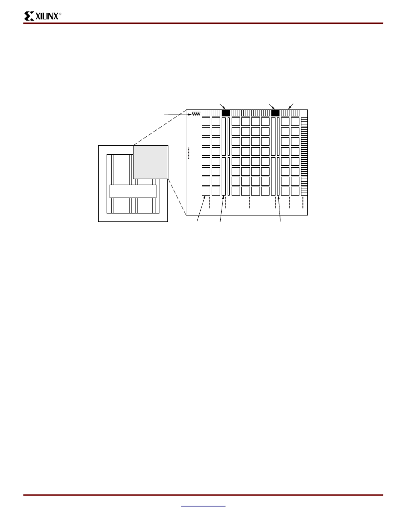
Virtex-II Array Overview
Virtex-II devices are user-programmable gate arrays with various configurable elements. The Virtex-II architecture is
optimized for high-density and high-performance logic designs. As shown in
Figure 1
, the programmable device is
comprised of input/output blocks (IOBs) and internal configurable logic blocks (CLBs).
Programmable I/O blocks provide the interface between
package pins and the internal configurable logic. Most
popular and leading-edge I/O standards are supported by
the programmable IOBs.
The internal configurable logic includes four major elements
organized in a regular array.
Configurable Logic Blocks (CLBs) provide functional
elements for combinatorial and synchronous logic,
including basic storage elements. BUFTs (3-state
buffers) associated with each CLB element drive
dedicated segmentable horizontal routing resources.
Block SelectRAM memory modules provide large
18-Kbit storage elements of True Dual-Port RAM.
Multiplier blocks are 18-bit x 18-bit dedicated
multipliers.
DCM (Digital Clock Manager) blocks provide
self-calibrating, fully digital solutions for clock
distribution delay compensation, clock multiplication
and division, coarse and fine-grained clock phase
shifting.
A new generation of programmable routing resources called
Active Interconnect Technology interconnects all of these
elements. The general routing matrix (GRM) is an array of
routing switches. Each programmable element is tied to a
switch matrix, allowing multiple connections to the general
routing matrix. The overall programmable interconnection is
hierarchical and designed to support high-speed designs.
All
resources, are controlled by values stored in static memory
cells. These values are loaded in the memory cells during
configuration and can be reloaded to change the functions
of the programmable elements.
programmable
elements,
including
the
routing
Virtex-II Features
This section briefly describes Virtex-II features.
Input/Output Blocks (IOBs)
IOBs are programmable and can be categorized as follows:
Input block with an optional single-data-rate or
double-data-rate (DDR) register
Output block with an optional single-data-rate or DDR
register, and an optional 3-state buffer, to be driven
directly or through a single or DDR register
Bi-directional block (any combination of input and
output configurations)
These registers are either edge-triggered D-type flip-flops
or level-sensitive latches.
IOBs support the following single-ended I/O standards:
LVTTL, LVCMOS (3.3 V, 2.5 V, 1.8 V, and 1.5 V)
PCI-X at 133 MHz, PCI (3.3 V at 33 MHz and 66 MHz)
GTL and GTLP
HSTL (Class I, II, III, and IV)
Figure 1:
Virtex-II
Architecture Overview
Global Clock Mux
DCM
DCM
IOB
CLB
Programmable I/Os
Block SelectRAM
Multiplier
Configurable Logic
DS031_28_100900
相關(guān)PDF資料 |
PDF描述 |
|---|---|
| XC2V4000-4FF1152I | Virtex-II 1.5V Field-Programmable Gate Arrays |
| XC2V2000-5FG676I | Virtex-II 1.5V Field-Programmable Gate Arrays |
| XC2V2000-4BG575I | Virtex-II 1.5V Field-Programmable Gate Arrays |
| XC2V2000-5BG575I | Virtex-II 1.5V Field-Programmable Gate Arrays |
| XC2V500-4FG256C | Virtex-II 1.5V Field-Programmable Gate Arrays |
相關(guān)代理商/技術(shù)參數(shù) |
參數(shù)描述 |
|---|---|
| XC2V500-4BF957C | 制造商:XILINX 制造商全稱:XILINX 功能描述:Virtex-II 1.5V Field-Programmable Gate Arrays |
| XC2V500-4BF957I | 制造商:XILINX 制造商全稱:XILINX 功能描述:Virtex-II 1.5V Field-Programmable Gate Arrays |
| XC2V500-4BG575C | 制造商:XILINX 制造商全稱:XILINX 功能描述:Virtex-II 1.5V Field-Programmable Gate Arrays |
| XC2V500-4BG575I | 制造商:XILINX 制造商全稱:XILINX 功能描述:Virtex-II 1.5V Field-Programmable Gate Arrays |
| XC2V500-4BG728C | 制造商:XILINX 制造商全稱:XILINX 功能描述:Virtex-II 1.5V Field-Programmable Gate Arrays |
發(fā)布緊急采購,3分鐘左右您將得到回復(fù)。