- 您現(xiàn)在的位置:買賣IC網(wǎng) > PDF目錄374970 > XC2V10000 (Xilinx, Inc.) Virtex-II 1.5V Field-Programmable Gate Arrays(Virtex-II 1.5V 現(xiàn)場(chǎng)可編程門陣列) PDF資料下載
參數(shù)資料
| 型號(hào): | XC2V10000 |
| 廠商: | Xilinx, Inc. |
| 英文描述: | Virtex-II 1.5V Field-Programmable Gate Arrays(Virtex-II 1.5V 現(xiàn)場(chǎng)可編程門陣列) |
| 中文描述: | 的Virtex - II 1.5V的現(xiàn)場(chǎng)可編程門陣列(的Virtex - II 1.5V的現(xiàn)場(chǎng)可編程門陣列) |
| 文件頁數(shù): | 2/8頁 |
| 文件大?。?/td> | 167K |
| 代理商: | XC2V10000 |
Module n of 4
2
1-800-255-7778Advance Product SpecificationVirtex-II 1.5V Field-Programmable Gate Arrays
R
General Description
The Virtex-II family is a platform FPGA developed for high performance from low-density to high-
density designs that are based on IP cores and customized modules. The family delivers complete
solutions for telecommunication, wireless, networking, video, and DSP applications, including PCI,
LVDS, and DDR interfaces.
The leading-edge 0.15μm / 0.12μm CMOS 8-layer metal process and the Virtex-II architecture are
optimized for high speed with low power consumption. Combining a wide variety of flexible features
and a large range of densities up to 10 million system gates, the Virtex-II family enhances
programmable logic design capabilities and is a powerful alternative to mask-programmed gates
arrays. As shown in
Table 1
, the Virtex-II family comprises 12 members, ranging from 40K to 10M
system gates.
Packaging
Offerings include ball grid array (BGA) packages with 0.80mm, 1.00mm, and 1.27mm pitches. In
addition to traditional wire-bond interconnects, flip-chip interconnect is used in some of the BGA
offerings. The use of flip-chip interconnect offers more I/Os than is possible in wire-bond versions of
the similar packages. Flip-Chip construction offers the combination of high pin count with high
thermal capacity.
Table 2
shows the maximum number of user I/Os available. The Virtex-II device/package
combination table (
Table 6
at the end of this section) details the maximum number of I/Os for each
device and package using wire-bond or flip-chip technology.
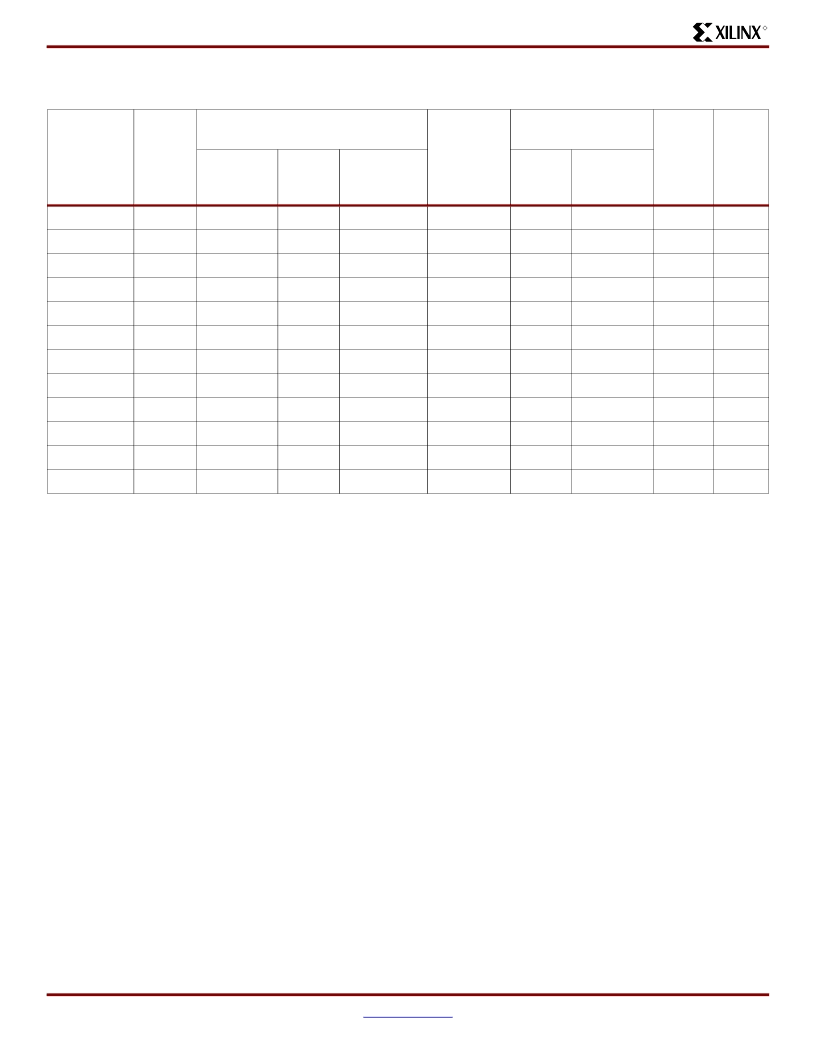
Table 1:
Virtex-II
Field-Programmable Gate Array Family Members
Device
System
Gates
CLB
(1 CLB = 4 slices = Max 128 bits)
Multiplier
Blocks
SelectRAM Blocks
DCMs
Max I/O
Pads
Array
Row x Col.
Slices
Maximum
Distributed
RAM Kbits
18-Kbit
Blocks
Max RAM
(Kbits)
XC2V40
40K
8 x 8
256
8
4
4
72
4
88
XC2V80
80K
16 x 8
512
16
8
8
144
4
120
XC2V250
250K
24 x 16
1,536
48
24
24
432
8
200
XC2V500
500K
32 x 24
3,072
96
32
32
576
8
264
XC2V1000
1M
40 x 32
5,120
160
40
40
720
8
432
XC2V1500
1.5M
48 x 40
7,680
240
48
48
864
8
528
XC2V2000
2M
56 x 48
10,752
336
56
56
1,008
8
624
XC2V3000
3M
64 x 56
14,336
448
96
96
1,728
12
720
XC2V4000
4M
80 x 72
23,040
720
120
120
2,160
12
912
XC2V6000
6M
96 x 88
33,792
1,056
144
144
2,592
12
1,104
XC2V8000
8M
112 x 104
46,592
1,456
168
168
3,024
12
1,108
XC2V10000
10M
128 x 120
61,440
1,920
192
192
3,456
12
1,108
相關(guān)PDF資料 |
PDF描述 |
|---|---|
| XC2V2000 | Virtex-II 1.5V Field-Programmable Gate Arrays(Virtex-II 1.5V 現(xiàn)場(chǎng)可編程門陣列) |
| XC2V1500 | Virtex-II 1.5V Field-Programmable Gate Arrays(Virtex-II 1.5V 現(xiàn)場(chǎng)可編程門陣列) |
| XC2V1000 | Virtex-II Platform FPGAs: Complete Data Sheet |
| XC2V1000-4FG456C | Virtex-II Platform FPGAs: Complete Data Sheet |
| XC2V1000-4FG456I | Virtex-II Platform FPGAs: Complete Data Sheet |
相關(guān)代理商/技術(shù)參數(shù) |
參數(shù)描述 |
|---|---|
| XC2V1000-4BF957C | 制造商:XILINX 制造商全稱:XILINX 功能描述:Virtex-II 1.5V Field-Programmable Gate Arrays |
| XC2V1000-4BF957I | 制造商:XILINX 制造商全稱:XILINX 功能描述:Virtex-II 1.5V Field-Programmable Gate Arrays |
| XC2V1000-4BG575C | 制造商:Xilinx 功能描述:FPGA VIRTEX-II 1M GATES 11520 CELLS 650MHZ 0.15UM/0.12UM 1.5 - Trays |
| XC2V1000-4BG575CES | 制造商:Xilinx 功能描述: |
| XC2V1000-4BG575I | 功能描述:IC FPGA VIRTEX-II 575PBGA RoHS:否 類別:集成電路 (IC) >> 嵌入式 - FPGA(現(xiàn)場(chǎng)可編程門陣列) 系列:Virtex®-II 產(chǎn)品變化通告:Step Intro and Pkg Change 11/March/2008 標(biāo)準(zhǔn)包裝:1 系列:Virtex®-5 SXT LAB/CLB數(shù):4080 邏輯元件/單元數(shù):52224 RAM 位總計(jì):4866048 輸入/輸出數(shù):480 門數(shù):- 電源電壓:0.95 V ~ 1.05 V 安裝類型:表面貼裝 工作溫度:-40°C ~ 100°C 封裝/外殼:1136-BBGA,F(xiàn)CBGA 供應(yīng)商設(shè)備封裝:1136-FCBGA 配用:568-5088-ND - BOARD DEMO DAC1408D750122-1796-ND - EVALUATION PLATFORM VIRTEX-5 |
發(fā)布緊急采購(gòu),3分鐘左右您將得到回復(fù)。