- 您現(xiàn)在的位置:買賣IC網(wǎng) > PDF目錄374964 > XC1700E (Xilinx, Inc.) Configuration PROMs PDF資料下載
參數(shù)資料
| 型號(hào): | XC1700E |
| 廠商: | Xilinx, Inc. |
| 英文描述: | Configuration PROMs |
| 中文描述: | 配置PROM的 |
| 文件頁數(shù): | 8/12頁 |
| 文件大小: | 124K |
| 代理商: | XC1700E |
R
XC1704L, XC1702L, XC1701L, XC17512L, XC1765EL, XC17128EL and XC17256EL
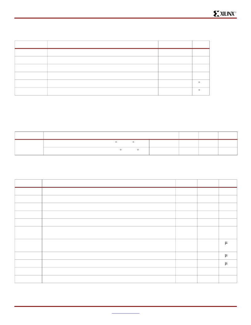
Absolute Maximum Ratings
Operating Conditions (3V Supply)
DC Characteristics Over Operating Condition
Symbol
Description
Conditions
Units
V
CC
Supply voltage relative to GND
–
0.5 to +7.0
V
V
PP
Supply voltage relative to GND
–
0.5 to +12.5
V
V
IN
Input voltage relative to GND
–
0.5 to V
CC
+0.5
V
V
TS
Voltage applied to High-Z output
–
0.5 to V
CC
+0.5
V
T
STG
Storage temperature (ambient)
–
65 to +150
°
C
T
SOL
Maximum soldering temperature (10s @ 1/16 in.)
+260
°
C
Notes:
1.
Stresses beyond those listed under Absolute Maximum Ratings may cause permanent damage to the device.
These are stress ratings only, and functional operation of the device at these or any other conditions beyond those
listed under Operating Conditions is not implied. Exposure to Absolute Maximum Ratings conditions for extended
periods of time may affect device reliability.
Symbol
Description
Min
Max
Units
V
CC(1)
Supply voltage relative to GND (T
A
= 0
°
C to +70
°
C)
Commercial
3.0
3.6
V
Supply voltage relative to GND (T
A
=
–
40
°
C to +85
°
C)
Industrial
3.0
3.6
V
Notes:
1.
During normal read operation V
PP
MUST
be connect to V
CC.
Symbol
Description
Min
Max
Units
V
IH
High-level input voltage
2
V
CC
V
V
IL
Low-level input voltage
0
0.8
V
V
OH
High-level output voltage (I
OH
=
–
3 mA)
2.4
-
V
V
OL
Low-level output voltage (I
OL
= +3 mA)
-
0.4
V
I
CCA
Supply current, active mode (at maximum frequency) (XC1700L)
-
10
mA
I
CCA
Supply current, active mode (at maximum frequency)
(XC1765EL, XC17128EL, XC17256EL)
-
5
mA
I
CCS
Supply current, standby mode (XC1701L, XC17512L, XC17256L,
X1765EL, XC17128EL)
-
50
m
A
I
CCS
Supply current, standby mode (XC1702L, XC1704L)
-
350
m
A
I
L
Input or output leakage current
–
10
10
m
A
C
IN
Input capacitance (V
IN
= GND, f = 1.0 MHz)
-
10
pF
C
OUT
Output capacitance (V
IN
= GND, f = 1.0 MHz)
-
10
pF
相關(guān)PDF資料 |
PDF描述 |
|---|---|
| XC1701LPC20C | Configuration PROMs |
| XC1701LPC20I | Configuration PROMs |
| XC1701LPD8C | Configuration PROMs |
| XC1701LSO20C | Configuration PROMs |
| XC1701LSO20I | Configuration PROMs |
相關(guān)代理商/技術(shù)參數(shù) |
參數(shù)描述 |
|---|---|
| XC1700E_1 | 制造商:XILINX 制造商全稱:XILINX 功能描述:Configuration PROMs |
| XC1700EL | 制造商:XILINX 制造商全稱:XILINX 功能描述:Configuration PROMs |
| XC1700ESERIES | 制造商:未知廠家 制造商全稱:未知廠家 功能描述:Configuration PROMs |
| XC1700L | 制造商:XILINX 制造商全稱:XILINX 功能描述:Configuration PROMs |
| XC1700LSERIES | 制造商:未知廠家 制造商全稱:未知廠家 功能描述:Configuration PROMs |
發(fā)布緊急采購,3分鐘左右您將得到回復(fù)。