- 您現(xiàn)在的位置:買賣IC網(wǎng) > PDF目錄382605 > TLC393Q (Texas Instruments, Inc.) DUAL MICROPOWER LinCMOSE VOLTAGE COMPARATOR PDF資料下載
參數(shù)資料
| 型號(hào): | TLC393Q |
| 廠商: | Texas Instruments, Inc. |
| 英文描述: | DUAL MICROPOWER LinCMOSE VOLTAGE COMPARATOR |
| 中文描述: | 雙微功耗電壓比較LinCMOSE |
| 文件頁數(shù): | 8/23頁 |
| 文件大小: | 354K |
| 代理商: | TLC393Q |
TLC193, TLC393
DUAL MICROPOWER LinCMOS
VOLTAGE COMPARATOR
SLCS115D – DECEMBER 1986 – REVISED JANUARY 1999
8
POST OFFICE BOX 655303
DALLAS, TEXAS 75265
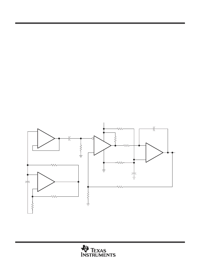
PARAMETER MEASUREMENT INFORMATION
A close approximation of the input offset voltage can be obtained by using a binary search method to vary the
differential input voltage while monitoring the output state. When the applied input voltage differential is equal,
but opposite in polarity, to the input offset voltage, the output changes states.
Figure 2 illustrates a practical circuit for direct dc measurement of input offset voltage that does not bias the
comparator in the linear region. The circuit consists of a switching-mode servo loop in which U1A generates
a triangular waveform of approximately 20-mV amplitude. U1B acts as a buffer, with C2 and R4 removing any
residual dc offset. The signal is then applied to the inverting input of the comparator under test, while the
noninverting input is driven by the output of the integrator formed by U1C through the voltage divider formed
by R9 and R10. The loop reaches a stable operating point when the output of the comparator under test has
a duty cycle of exactly 50%, which can only occur when the incoming triangle wave is sliced symmetrically or
when the voltage at the noninverting input exactly equals the input offset voltage.
The voltage divider formed by R9 and R10 provides an increase in input offset voltage by a factor of 100 to
make measurement easier. The values of R5, R8, R9, and R10 can significantly influence the accuracy of the
reading; therefore, it is suggested that their tolerance level be 1% or lower.
Measuring the extremely low values of input current requires isolation from all other sources of leakage current
and compensation for the leakage of the test socket and board. With a good picoammeter, the socket and board
leakage can be measured with no device in the socket. Subsequently, this open-socket leakage value can be
subtracted from the measurement obtained with a device in the socket to obtain the actual input current of the
device.
–
+
DUT
VDD
+
–
–
+
–
+
C2
1
μ
F
R4
47 k
R5
1.8 k
,
1%
C3
0.68
μ
F
U1C
1/4 TLC274CN
U1B
1/4 TLC274CN
U1A
1/4 TLC274CN
R7
1 M
R8
1.8 k
,
1%
R9
10 k
,
1%
R1
240 k
R2
10 k
C1
0.1
μ
F
R3
100
C4
0.1
μ
F
Integrator
R10
100
,
1%
Buffer
Triangle
Generator
VIO
(X100)
R6
5.1 k
Figure 2. Circuit for Input Offset Voltage Measurement
相關(guān)PDF資料 |
PDF描述 |
|---|---|
| TLC193D | DUAL MICROPOWER LinCMOSE VOLTAGE COMPARATOR |
| TLC193FK | DUAL MICROPOWER LinCMOSE VOLTAGE COMPARATOR |
| TLC393JG | DUAL MICROPOWER LinCMOSE VOLTAGE COMPARATOR |
| TLC220xY | Advanced LinCMOSE LOW-NOISE PRECISION OPERATIONAL AMPLIFIERS |
| TLC2201BMFK | Advanced LinCMOSE LOW-NOISE PRECISION OPERATIONAL AMPLIFIERS |
相關(guān)代理商/技術(shù)參數(shù) |
參數(shù)描述 |
|---|---|
| TLC393-Q1 | 制造商:TI 制造商全稱:Texas Instruments 功能描述:DUAL MICROPOWER LinCMOS?£a VOLTAGE COMPARATOR |
| TLC393QD | 制造商:TI 制造商全稱:Texas Instruments 功能描述:DUAL MICROPOWER LinCMOSE VOLTAGE COMPARATOR |
| TLC393QDR | 功能描述:校驗(yàn)器 IC Dual Micropower LinCMOS Voltage RoHS:否 制造商:STMicroelectronics 產(chǎn)品: 比較器類型: 通道數(shù)量: 輸出類型:Push-Pull 電源電壓-最大:5.5 V 電源電壓-最小:1.1 V 補(bǔ)償電壓(最大值):6 mV 電源電流(最大值):1350 nA 響應(yīng)時(shí)間: 最大工作溫度:+ 125 C 安裝風(fēng)格:SMD/SMT 封裝 / 箱體:SC-70-5 封裝:Reel |
| TLC393QDRG4 | 功能描述:校驗(yàn)器 IC Dual McroPWR LinCMOS VLTG Comparator RoHS:否 制造商:STMicroelectronics 產(chǎn)品: 比較器類型: 通道數(shù)量: 輸出類型:Push-Pull 電源電壓-最大:5.5 V 電源電壓-最小:1.1 V 補(bǔ)償電壓(最大值):6 mV 電源電流(最大值):1350 nA 響應(yīng)時(shí)間: 最大工作溫度:+ 125 C 安裝風(fēng)格:SMD/SMT 封裝 / 箱體:SC-70-5 封裝:Reel |
| TLC393QDRG4Q1 | 功能描述:校驗(yàn)器 IC Dual McroPWR LinCMOS VLTG Comparator RoHS:否 制造商:STMicroelectronics 產(chǎn)品: 比較器類型: 通道數(shù)量: 輸出類型:Push-Pull 電源電壓-最大:5.5 V 電源電壓-最小:1.1 V 補(bǔ)償電壓(最大值):6 mV 電源電流(最大值):1350 nA 響應(yīng)時(shí)間: 最大工作溫度:+ 125 C 安裝風(fēng)格:SMD/SMT 封裝 / 箱體:SC-70-5 封裝:Reel |
發(fā)布緊急采購,3分鐘左右您將得到回復(fù)。