- 您現(xiàn)在的位置:買(mǎi)賣(mài)IC網(wǎng) > PDF目錄374939 > STF202-22TC (Semtech Corporation) USB Upstream Port Filter & TVS For EMI Filtering and ESD Protection PDF資料下載
參數(shù)資料
| 型號(hào): | STF202-22TC |
| 廠商: | Semtech Corporation |
| 英文描述: | USB Upstream Port Filter & TVS For EMI Filtering and ESD Protection |
| 中文描述: | 上游的USB端口過(guò)濾 |
| 文件頁(yè)數(shù): | 4/6頁(yè) |
| 文件大小: | 164K |
| 代理商: | STF202-22TC |
2000 SEMTECH CORP.
652 MITCHELL ROAD NEWBURY PARK CA 91320
Objective - March 03, 2000
USB Upstream Port Filter & TVS
For EMI Filtering and ESD Protection
STF202-22
&
STF202-30
APPLICATIONS INFORMATION
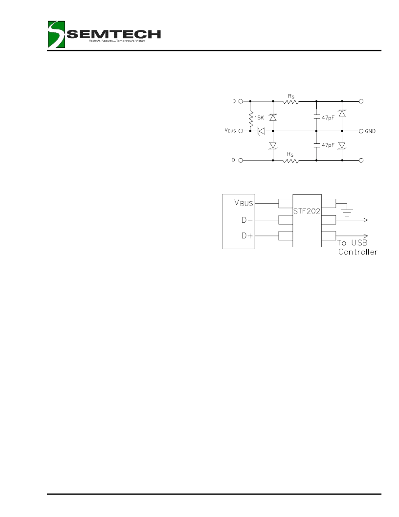
Figure 1 - STF202 Circuit Diagram
Device Connection
The STF202 is designed to provide termination, EMI
filtering and ESD protection for two USB I/O lines. The
equivalent circuit diagram is shown in Figure 1. The
device is connected as follows:
1. Full-Speed Devices:
For full-speed devices the
pull-up resistor is connected to the D+ line. Pin 1
is connected to the voltage supply line (V
BUS
). The
input of the D+ line is routed into pin 3 and out of
pin 4. The input of the D- line is connected at pin 2
and the output at pin 5. Pin 6 is connected to
ground.
Low-Speed Devices:
For low speed devices the
pull-up resistor is connected to the D- line. Pins 1
is connected to the voltage supply line (V
BUS
). The
input of the D- line is connected at pin 3 with the
output taken at pin 4. The input of the D+ line is
connected to pin 2 and the output is at pin 5. Pin 6
is connected to ground.
USB Port Design Considerations
The Universal Serial Bus (USB) specification requires
termination and filtering components for proper
operation. In addition, an open USB socket is
vulnerable to hazardous ESD discharges in excess of
15kV. These discharges can may occur on the data
lines or the voltage bus. The STF202 is an easily
implemented solution designed to meet the termination
& EMI filter requirements of the USB specification
revision 1.1. It also provides ESD protection to IEC
61000-4-2, level 4.
A simplified USB port is shown in Figure 3. USB line
termination is achieved with series resistors on both the
D+ and D- lines. These resistors preserve signal
integrity by matching the cable impedance to that of the
differential driver. 15k
pull-down resistors are used to
identify a downstream port while an upstream port is
identified with a 1.5K
pull up resistor on either the D+
(full speed devices) or the D- (low speed devices) data
line. Capacitors are used to bypass high frequency
energy to ground and for edge rate control of the USB
signals. TVS diodes are added for ESD protection of
both (D+ & D-) data lines and the voltage bus (V
BUS
). A
power distribution switch and voltage regulator provide
the power management functions of the port.
Semtech provides a complete solution to simplify USB
port design (Figure 4). The STF201 & STF202
Figure 2 - STF202 Connection Diagram
(Full Speed Devices)
1
2
3
4
5
6
integrate all of the components necessary for line
termination, bidirectional EMI filtering, and ESD
protection on downstream (STF201) or upstream
(STF202) ports. The SC5826 is a dual port power
switch that provides individual or ganged port
switching, fault reporting, and inrush current limiting as
required by the USB specification. The SC5205 ULDO
provides a stable voltage to the USB controller.
Board Placement & Layout Guidelines.
Designing a USB hub to meet EMI & ESD immunity
requirements requires a combination of optimum
component placement, trace routing, and good circuit
design practices. Some general guidelines are given
below:
Avoid running D+ & D- signal line traces near high
speed clock lines or similar signal lines.
Avoid running critical signal lines near board
edges.
Locate the USB controller chip near the USB
connectors.
Place the STF202 near the USB connector to
restrict transient coupling.
Minimize the path length between the USB
connector and the STF202
.
相關(guān)PDF資料 |
PDF描述 |
|---|---|
| STF202-30 | USB Upstream Port Filter & TVS For EMI Filtering and ESD Protection |
| STF202-30TC | USB Upstream Port Filter & TVS For EMI Filtering and ESD Protection |
| STF701 | T-Filter with TVS Diode Array For EMI Filtering and ESD Protection |
| STF701TC | T-Filter with TVS Diode Array For EMI Filtering and ESD Protection |
| STF701TG | T-Filter with TVS Diode Array For EMI Filtering and ESD Protection |
相關(guān)代理商/技術(shù)參數(shù) |
參數(shù)描述 |
|---|---|
| STF202-30 | 制造商:SEMTECH 制造商全稱:Semtech Corporation 功能描述:USB Upstream Port Filter & TVS For EMI Filtering and ESD Protection |
| STF202-30.TC | 制造商:Semtech Corporation 功能描述:EMI Filter Gull Wing SMD 制造商:Semtech Corporation 功能描述:1 FUNCTIONS, 6 V, DATA LINE FILTER |
| STF202-30.TCT | 制造商:Semtech Corporation 功能描述:EMI Filter Gull Wing SMD T/R 制造商:Semtech Corporation 功能描述:USB UP-STREAM PORT FILTER & TVS / LEAD-F |
| STF202-30TC | 制造商:SEMTECH 制造商全稱:Semtech Corporation 功能描述:USB Upstream Port Filter & TVS For EMI Filtering and ESD Protection |
| STF203-15 | 制造商:SEMTECH 制造商全稱:Semtech Corporation 功能描述:USB Upstream Port Filter and TVS |
發(fā)布緊急采購(gòu),3分鐘左右您將得到回復(fù)。