- 您現在的位置:買賣IC網 > PDF目錄374928 > SSD1815T1R (Electronic Theatre Controls, Inc.) SEMICONDUCTOR TECHNICAL DATA PDF資料下載
參數資料
| 型號: | SSD1815T1R |
| 廠商: | Electronic Theatre Controls, Inc. |
| 英文描述: | SEMICONDUCTOR TECHNICAL DATA |
| 中文描述: | 半導體技術數據 |
| 文件頁數: | 19/35頁 |
| 文件大?。?/td> | 856K |
| 代理商: | SSD1815T1R |
第1頁第2頁第3頁第4頁第5頁第6頁第7頁第8頁第9頁第10頁第11頁第12頁第13頁第14頁第15頁第16頁第17頁第18頁當前第19頁第20頁第21頁第22頁第23頁第24頁第25頁第26頁第27頁第28頁第29頁第30頁第31頁第32頁第33頁第34頁第35頁
S OLOMON
SSD1815
19
REV 1.5
03/2000
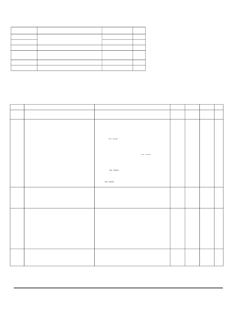
MAXIMUM RATINGS*
(Voltages Referenced to V
SS
)
Symbol
Parameter
Value
Unit
V
DD
V
EE
V
in
I
Supply Voltage
-0.3 to +4.0
V
0 to -12.0
V
Input Voltage
V
SS
-0.3 to V
DD
+0.3
25
V
Current Drain Per Pin Excluding V
DD
and
V
SS
Operating Temperature
mA
T
A
T
stg
-30 to +85
°C
Storage Temperature Range
-65 to +150
°C
* Maximum Ratings are those values beyond which damage to the device may occur. Functional
operation should be restricted to the limits in the Electrical Characteristics tables or Pin Descrip-
tion section.
This device contains circuitry to protect the inputs
against damage due to high static voltages or elec-
tric fields; however, it is advised that normal precau-
tions to be taken to avoid application of any voltage
higher than maximum rated voltages to this high
impedance circuit. For proper operation it is recom-
mended that V
in
and V
out
be constrained to the
range V
SS
< or = (V
in
or V
out
) < or = V
DD
. Reliability
of operation is enhanced if unused input are con-
nected to an appropriate logic voltage level (e.g.,
either V
SS
or V
DD
). Unused outputs must be left
open. This device may be light sensitive. Caution
should be taken to avoid exposure of this device to
any light source during normal operation. This
device is not radiation protected.
DC CHARACTERISTICS
(Unless otherwise specified, Voltage Referenced to V
SS
, V
DD
= 2.4 to 3.5V, T
A
= -30 to 85°C.)
Symbol
Parameter
Test Condition
Min
Typ
Max
Unit
V
DD
Logic Circuit Supply Voltage Range
Recommend Operating Voltage
Possible Operating Voltage
2.4
1.8
2.7
-
3.5
3.5
V
V
I
AC
I
DP1
I
DP2
I
SB
I
SLEEP
Access Mode Supply Current Drain (V
DD
Pins)
Display Mode Supply Current Drain (V
DD
Pins)
Display Mode Supply Current Drain (V
DD
Pins)
Standby Mode Supply Current Drain (V
DD
Pins)
Sleep Mode Supply Current Drain (V
DD
Pins)
V
DD
= 2.7V, Voltage Generator On, 4X DC-DC Con-
verter Enabled, Write accessing, T
cyc
=3.3MHz, Osc.
Freq.=17kHz, Display On.
V
DD
= 2.7V, V
EE
= -8.1V, Voltage Generator Dis-
abled, R/W(WR) Halt, Osc. Freq. = 17kHz, Display
On, V
L6
- V
DD
= -8.1V.
V
DD
= 2.7V, V
EE
= -8.1V, Voltage Generator On, 4x
DC-DC Converter Enabled, R/W(WR) Halt, Osc.
Freq. = 17kHz, Display On, V
L6
- V
DD
= -8.1V.
V
DD
=2.7V, LCD Driving Waveform Off, Osc. Freq. =
17kHz, R/W(WR) halt.
V
DD
= 2.7V, LCD Driving Waveform Off, Oscillator
Off, R/W(WR) halt.
-
-
-
-
-
300
60
150
3.5
0.2
600
100
200
10
5
μ
A
μ
A
μ
A
μ
A
μ
A
V
EE
V
LCD
V
OH1
LCD Driving Voltage Generator Output (V
EE
Pin)
LCD Driving Voltage Input (V
EE
Pin)
Logic High Output Voltage
Display On, Voltage Generator Enabled, DC/DC
Converter Enabled, Osc. Freq.=17kHz, Regulator
Enabled, Divider Enabled.
Voltage Generator Disabled.
-12.0
-12.0
-
-
-1.8
-1.8
V
V
V
OL1
V
L6
V
L6
V
IH1
Logic Low Output Voltage
LCD Driving Voltage Source (V
L6
Pin)
LCD Driving Voltage Source (V
L6
Pin)
Logic High Input voltage
I
out
=100
μ
A
I
out
=100
μ
A
Regulator Enabled (V
L6
voltage depends on Int/Ext
Contrast Control)
Regulator Disable
0.9*V
DD
0
V
EE
-0.5
-
-
-
-
Floating
V
DD
0.1*V
DD
V
DD
-
V
V
V
V
V
IL1
Logic Low Input voltage
0.8*V
DD
0
-
-
V
DD
0.2*V
DD
V
V
相關PDF資料 |
PDF描述 |
|---|---|
| SSD1815T2R | SEMICONDUCTOR TECHNICAL DATA |
| SSD1815T3R | SEMICONDUCTOR TECHNICAL DATA |
| SSD1815TR | SEMICONDUCTOR TECHNICAL DATA |
| SSD1815Z | SEMICONDUCTOR TECHNICAL DATA |
| SSD1818A | LCD Segment / Common Driver with Controller |
相關代理商/技術參數 |
參數描述 |
|---|---|
| SSD1815T2R | 制造商:未知廠家 制造商全稱:未知廠家 功能描述:SEMICONDUCTOR TECHNICAL DATA |
| SSD1815T3R | 制造商:未知廠家 制造商全稱:未知廠家 功能描述:SEMICONDUCTOR TECHNICAL DATA |
| SSD1815TR | 制造商:未知廠家 制造商全稱:未知廠家 功能描述:SEMICONDUCTOR TECHNICAL DATA |
| SSD1815Z | 制造商:未知廠家 制造商全稱:未知廠家 功能描述:SEMICONDUCTOR TECHNICAL DATA |
| SSD1818 | 制造商:未知廠家 制造商全稱:未知廠家 功能描述:LCD Segment / Common Driver with Controller |
發(fā)布緊急采購,3分鐘左右您將得到回復。