- 您現(xiàn)在的位置:買賣IC網(wǎng) > PDF目錄374928 > SSD1339U3 (Electronic Theatre Controls, Inc.) 132RGB x 132 with 2 smart Icon lines Dot Matrix OLED/PLED Segment/Common Driver with Controller PDF資料下載
參數(shù)資料
| 型號: | SSD1339U3 |
| 廠商: | Electronic Theatre Controls, Inc. |
| 英文描述: | 132RGB x 132 with 2 smart Icon lines Dot Matrix OLED/PLED Segment/Common Driver with Controller |
| 中文描述: | 132RGB × 132 2智能圖標(biāo)行點(diǎn)陣的OLED /短差段/驅(qū)動(dòng)器與控制器通用 |
| 文件頁數(shù): | 20/59頁 |
| 文件大小: | 916K |
| 代理商: | SSD1339U3 |
第1頁第2頁第3頁第4頁第5頁第6頁第7頁第8頁第9頁第10頁第11頁第12頁第13頁第14頁第15頁第16頁第17頁第18頁第19頁當(dāng)前第20頁第21頁第22頁第23頁第24頁第25頁第26頁第27頁第28頁第29頁第30頁第31頁第32頁第33頁第34頁第35頁第36頁第37頁第38頁第39頁第40頁第41頁第42頁第43頁第44頁第45頁第46頁第47頁第48頁第49頁第50頁第51頁第52頁第53頁第54頁第55頁第56頁第57頁第58頁第59頁
Solomon Systech
Jul 2005
P 20/59 Rev 1.1
SSD1339
Command Decoder and Command Interface
This module determines whether the input data is interpreted as data or command. Data is interpreted
based upon the input of the D/C# pin.
If D/C# pin is high, data is written to Graphic Display Data RAM (GDDRAM). If it is low, the input at D
7
-D
0
is interpreted as a Command and it will be decoded and be written to the corresponding command
register.
MPU Parallel 6800-series Interface
The parallel interface consists of 18 bi-directional data pins (D
17
-D
0
) or 8 bi-directional data pins (D
7
-D
0
),
R/W#(WR#), D/C#, E (RD#) and CS#. R/W#(WR#) input High indicates a read operation from the Graphic
Display Data RAM (GDDRAM) or the status register. RW#/(WR#) input Low indicates a write operation to
Display Data RAM or Internal Command Registers depending on the status of D/C# input. The E(RD#)
input serves as data latch signal (clock) when high provided that CS# is low and high respectively. Refer
to .
Figure 32 of parallel timing characteristics for Parallel Interface Timing Diagram of 6800-series
microprocessors.
In order to match the operating frequency of display RAM with that of the microprocessor, some pipeline
processing is internally performed which requires the insertion of a dummy read before the first actual
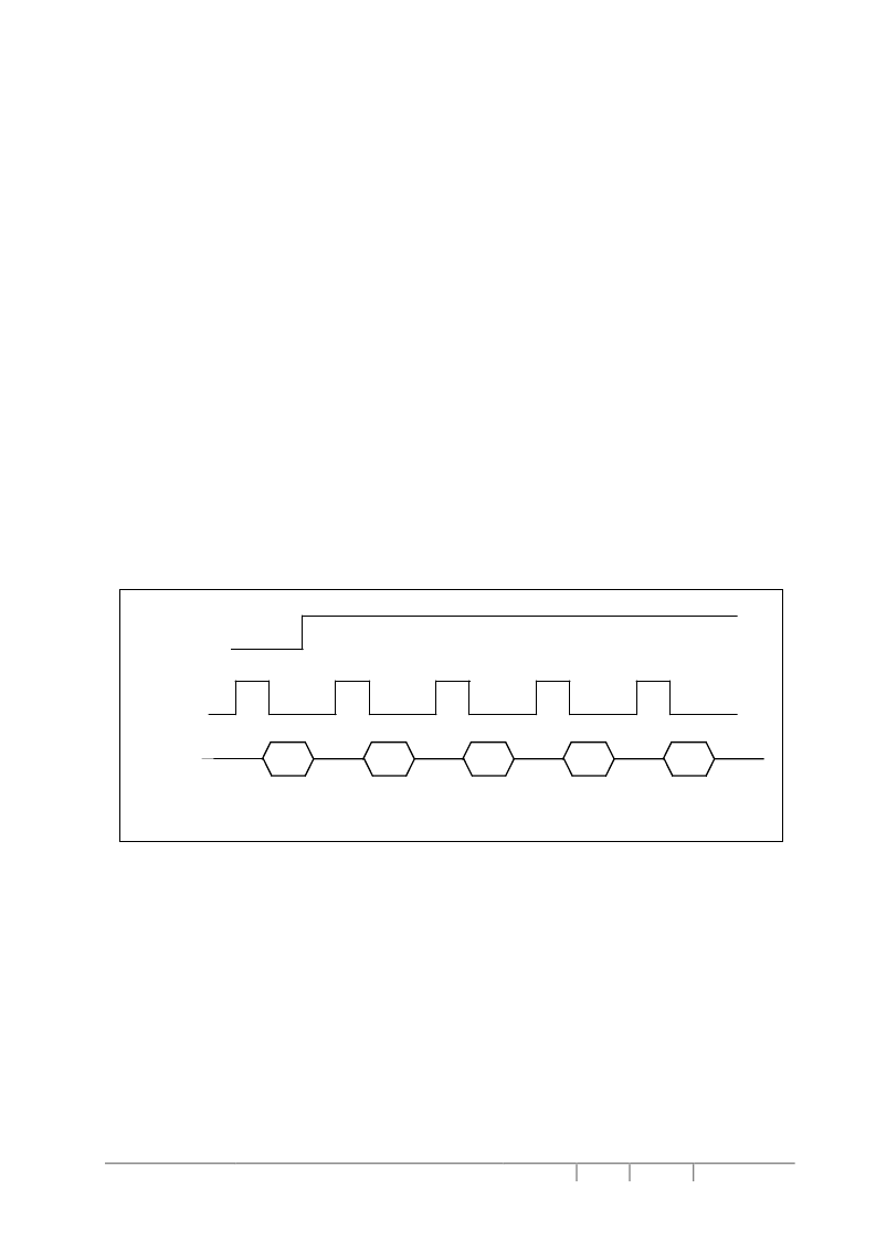
display data read. This is shown in Figure 6 below.
n+2
n+1
Write column
address
Dummy read
Data read1
R/
W#(WR#)
Data bus
N
n
E(RD#)
Data read2
Data read3
Figure 6 – Display data read back procedure - insertion of dummy read
MPU Parallel 8080-series Interface
The parallel interface consists of 18 bi-directional data pins (D
17
-D
0
) or 8 bi-directional data pins (D
7
-D
0
), E
(RD#), R/W#(WR#), D/C# and CS#. The E(RD#) input serves as data read latch signal (clock) when low,
provided that CS# is low and high respectively. Display data or status register read is controlled by D/C#.
R/W#(WR#) input serves as data write latch signal (clock) when high provided that CS# is low and high
respectively. Display data or command register write is controlled by D/C#. Refer to * when 8 bit used: D
0
~ D
7
instead; when 9 bit used: D
0
~ D
8
instead; when 16 bit used: D
0
~ D
15
instead; when 18 bit used: D
0
~ D
17
instead.
Figure 33 of parallel timing characteristics for Parallel Interface Timing Diagram of 8080-series
microprocessor. Similar to 6800-series interface, a dummy read is also required before the first actual
display data read.
相關(guān)PDF資料 |
PDF描述 |
|---|---|
| SSD1339Z | 132RGB x 132 with 2 smart Icon lines Dot Matrix OLED/PLED Segment/Common Driver with Controller |
| SSD1702T3R1 | 240-outputs LCD driver |
| SSD1702T2R1 | 240-outputs LCD driver |
| SSD1702 | 240-outputs LCD driver |
| SSD1702Z | 240-outputs LCD driver |
相關(guān)代理商/技術(shù)參數(shù) |
參數(shù)描述 |
|---|---|
| SSD1339Z | 制造商:未知廠家 制造商全稱:未知廠家 功能描述:132RGB x 132 with 2 smart Icon lines Dot Matrix OLED/PLED Segment/Common Driver with Controller |
| SSD1422 | 制造商:Hubbell Wiring Device-Kellems 功能描述:WALLPLATE, 1-G, D-HOLE, SS |
| SSD1423 | 制造商:Hubbell Wiring Device-Kellems 功能描述:WALLPLATE, 1-G, 2) D-HOLE, SS |
| SSD1428 | 制造商:Hubbell Wiring Device-Kellems 功能描述:WALLPLATE, 1-G, D-HOLE, SS |
| SSD1429 | 制造商:Hubbell Premise Wiring 功能描述: |
發(fā)布緊急采購,3分鐘左右您將得到回復(fù)。