- 您現(xiàn)在的位置:買賣IC網(wǎng) > PDF目錄374861 > SN74ACT3651PQ (Texas Instruments, Inc.) Low-Voltage CMOS Octal Transparent Latch; Package: TSSOP 20 LEAD; No of Pins: 20; Container: Tape and Reel; Qty per Container: 2500 PDF資料下載
參數(shù)資料
| 型號: | SN74ACT3651PQ |
| 廠商: | Texas Instruments, Inc. |
| 英文描述: | Low-Voltage CMOS Octal Transparent Latch; Package: TSSOP 20 LEAD; No of Pins: 20; Container: Tape and Reel; Qty per Container: 2500 |
| 中文描述: | 2048】36時(shí)鐘先入先出存儲(chǔ)器 |
| 文件頁數(shù): | 7/26頁 |
| 文件大?。?/td> | 376K |
| 代理商: | SN74ACT3651PQ |
第1頁第2頁第3頁第4頁第5頁第6頁當(dāng)前第7頁第8頁第9頁第10頁第11頁第12頁第13頁第14頁第15頁第16頁第17頁第18頁第19頁第20頁第21頁第22頁第23頁第24頁第25頁第26頁
SN74ACT3651
2048
×
36
CLOCKED FIRST-IN, FIRST-OUT MEMORY
SCAS439D – JUNE 1994 – REVISED FEBRUARY 1999
7
POST OFFICE BOX 655303
DALLAS, TEXAS 75265
serial load
To program the X and Y registers serially, the device is reset with FS0/SD and FS1/SEN high during the
low-to-high transition of RST. After this reset is complete, the X-and Y-register values are loaded bitwise through
FS0/SD on each low-to-high transition of CLKA that FS1/SEN is low. Twenty-two bit writes are needed to
complete the programming. The first bit write stores the most-significant bit of the Y register and the last bit write
stores the least-significant bit of the X register. Each register value can be programmed from 1 to 2044.
When the option is chosen to program the offset registers serially, the IR flag remains low until all register bits
are written. The IR flag is set high by the low-to-high transition of CLKA after the last bit is loaded, to allow normal
FIFO operation.
FIFO write/read operation
The state of the port-A data (A0–A35) outputs is controlled by the port-A chip select (CSA) and the port-A
write/read select (W/RA). The A0–A35 outputs are in the high-impedance state when either CSA or W/RA is
high. The A0–A35 outputs are active when both CSA and W/RA are low.
Data is loaded into the FIFO from the A0–A35 inputs on a low-to-high transition of CLKA when CSA and the
port-A mailbox select (MBA) are low, W/RA, the port-A enable (ENA), and the IR flag are high (see Table 2).
Writes to the FIFO are independent of any concurrent FIFO reads.
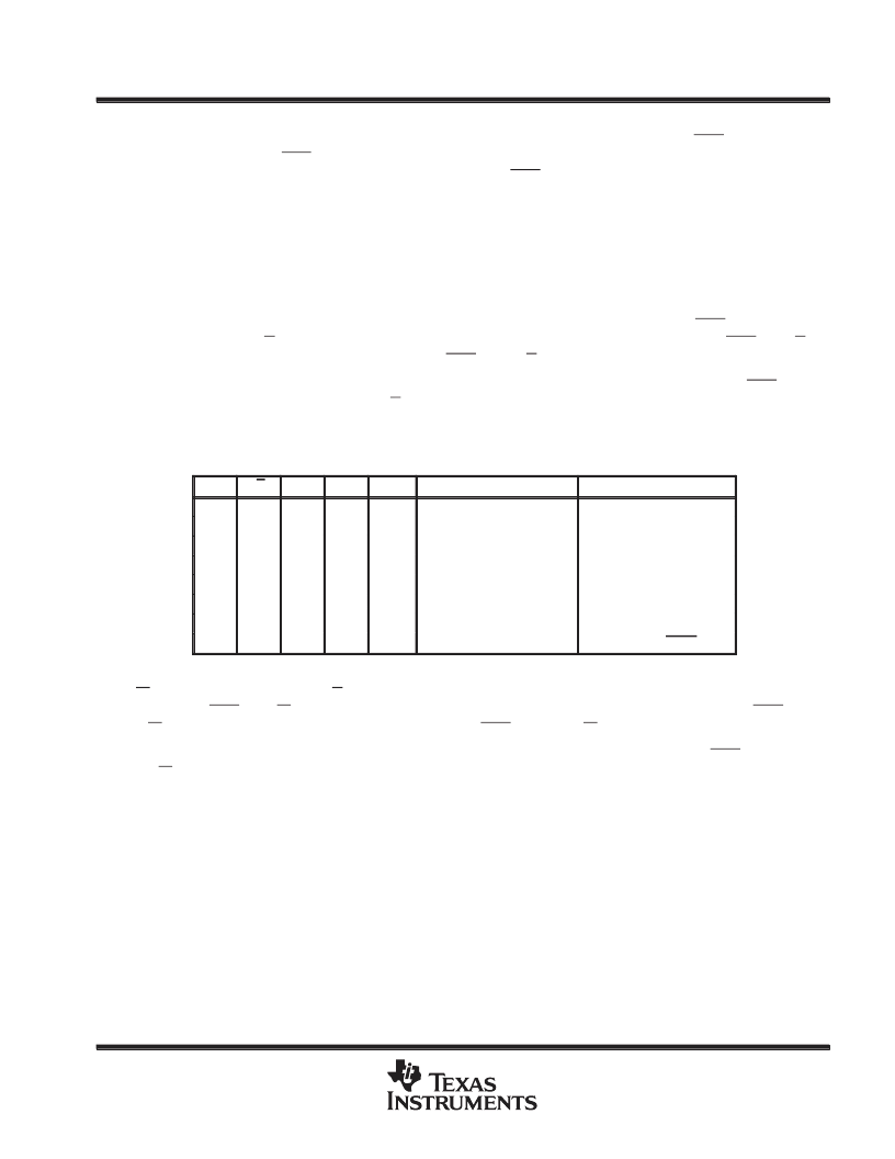
Table 2. Port-A Enable Function Table
CSA
W/RA
ENA
MBA
CLKA
A0–A35 OUTPUTS
In high-impedance state
In high-impedance state
In high-impedance state
In high-impedance state
Active, mail2 register
Active, mail2 register
Active, mail2 register
Active, mail2 register
PORT FUNCTION
None
None
FIFO write
Mail1 write
None
None
None
Mail2 read (set MBF2 high)
H
L
L
L
L
L
L
L
X
H
H
H
L
L
L
L
X
L
H
H
L
H
L
H
X
X
L
H
L
L
H
H
X
X
↑
↑
X
↑
X
↑
The port-B control signals are identical to those of port A, with the exception that the port-B write/read select
(W/RB) is the inverse of the W/RA. The state of the port-B data (B0–B35) outputs is controlled by the port-B
chip select (CSB) and W/RB. The B0–B35 outputs are in the high-impedance state when either CSB is high
or W/RB is low. The B0–B35 outputs are active when CSB is low and W/RB is high.
Data is read from the FIFO to its output register on a low-to-high transition of CLKB when CSB and MBB are
low, W/RB, ENB, and the OR flag are high (see Table 3). Reads from the FIFO are independent of any concurrent
FIFO writes.
相關(guān)PDF資料 |
PDF描述 |
|---|---|
| SN74ACT373DB | OCTAL D-TYPE TRANSPARENT LATCHES WITH 3-STATE OUTPUTS |
| SN54ACT373FK | OCTAL D-TYPE TRANSPARENT LATCHES WITH 3-STATE OUTPUTS |
| SN54ACT373J | OCTAL D-TYPE TRANSPARENT LATCHES WITH 3-STATE OUTPUTS |
| SN54ACT373W | OCTAL D-TYPE TRANSPARENT LATCHES WITH 3-STATE OUTPUTS |
| SN74ACT374DB | OCTAL D-TYPE EDGE-TRIGGERED FLIP-FLOPS WITH 3-STATE OUTPUTS |
相關(guān)代理商/技術(shù)參數(shù) |
參數(shù)描述 |
|---|---|
| SN74ACT373DB | 制造商:Rochester Electronics LLC 功能描述:- Bulk |
| SN74ACT373DBR | 功能描述:閉鎖 Tri-St Octal D-Type RoHS:否 制造商:Micrel 電路數(shù)量:1 邏輯類型:CMOS 邏輯系列:TTL 極性:Non-Inverting 輸出線路數(shù)量:9 高電平輸出電流: 低電平輸出電流: 傳播延遲時(shí)間: 電源電壓-最大:12 V 電源電壓-最小:5 V 最大工作溫度:+ 85 C 最小工作溫度:- 40 C 封裝 / 箱體:SOIC-16 封裝:Reel |
| SN74ACT373DBRE4 | 功能描述:閉鎖 Tri-St Octal D-Type RoHS:否 制造商:Micrel 電路數(shù)量:1 邏輯類型:CMOS 邏輯系列:TTL 極性:Non-Inverting 輸出線路數(shù)量:9 高電平輸出電流: 低電平輸出電流: 傳播延遲時(shí)間: 電源電壓-最大:12 V 電源電壓-最小:5 V 最大工作溫度:+ 85 C 最小工作溫度:- 40 C 封裝 / 箱體:SOIC-16 封裝:Reel |
| SN74ACT373DBRG4 | 功能描述:閉鎖 Octal D-Type Transp RoHS:否 制造商:Micrel 電路數(shù)量:1 邏輯類型:CMOS 邏輯系列:TTL 極性:Non-Inverting 輸出線路數(shù)量:9 高電平輸出電流: 低電平輸出電流: 傳播延遲時(shí)間: 電源電壓-最大:12 V 電源電壓-最小:5 V 最大工作溫度:+ 85 C 最小工作溫度:- 40 C 封裝 / 箱體:SOIC-16 封裝:Reel |
| SN74ACT373DW | 功能描述:閉鎖 Tri-St Octal D-Type RoHS:否 制造商:Micrel 電路數(shù)量:1 邏輯類型:CMOS 邏輯系列:TTL 極性:Non-Inverting 輸出線路數(shù)量:9 高電平輸出電流: 低電平輸出電流: 傳播延遲時(shí)間: 電源電壓-最大:12 V 電源電壓-最小:5 V 最大工作溫度:+ 85 C 最小工作溫度:- 40 C 封裝 / 箱體:SOIC-16 封裝:Reel |
發(fā)布緊急采購,3分鐘左右您將得到回復(fù)。