- 您現(xiàn)在的位置:買賣IC網(wǎng) > PDF目錄374851 > SN54BCT573W (Texas Instruments, Inc.) OCTAL TRANSPARENT D-TYPE LATCHES WITH 3-STATE OUTPUTS PDF資料下載
參數(shù)資料
| 型號: | SN54BCT573W |
| 廠商: | Texas Instruments, Inc. |
| 英文描述: | OCTAL TRANSPARENT D-TYPE LATCHES WITH 3-STATE OUTPUTS |
| 中文描述: | 有三態(tài)輸出的8個透明D型鎖存器 |
| 文件頁數(shù): | 2/5頁 |
| 文件大小: | 73K |
| 代理商: | SN54BCT573W |
SN54BCT573, SN74BCT573
OCTAL TRANSPARENT D-TYPE LATCHES
WITH 3-STATE OUTPUTS
SCBS071A – AUGUST 1990 – REVISED NOVEMBER 1993
2–2
POST OFFICE BOX 655303
DALLAS, TEXAS 75265
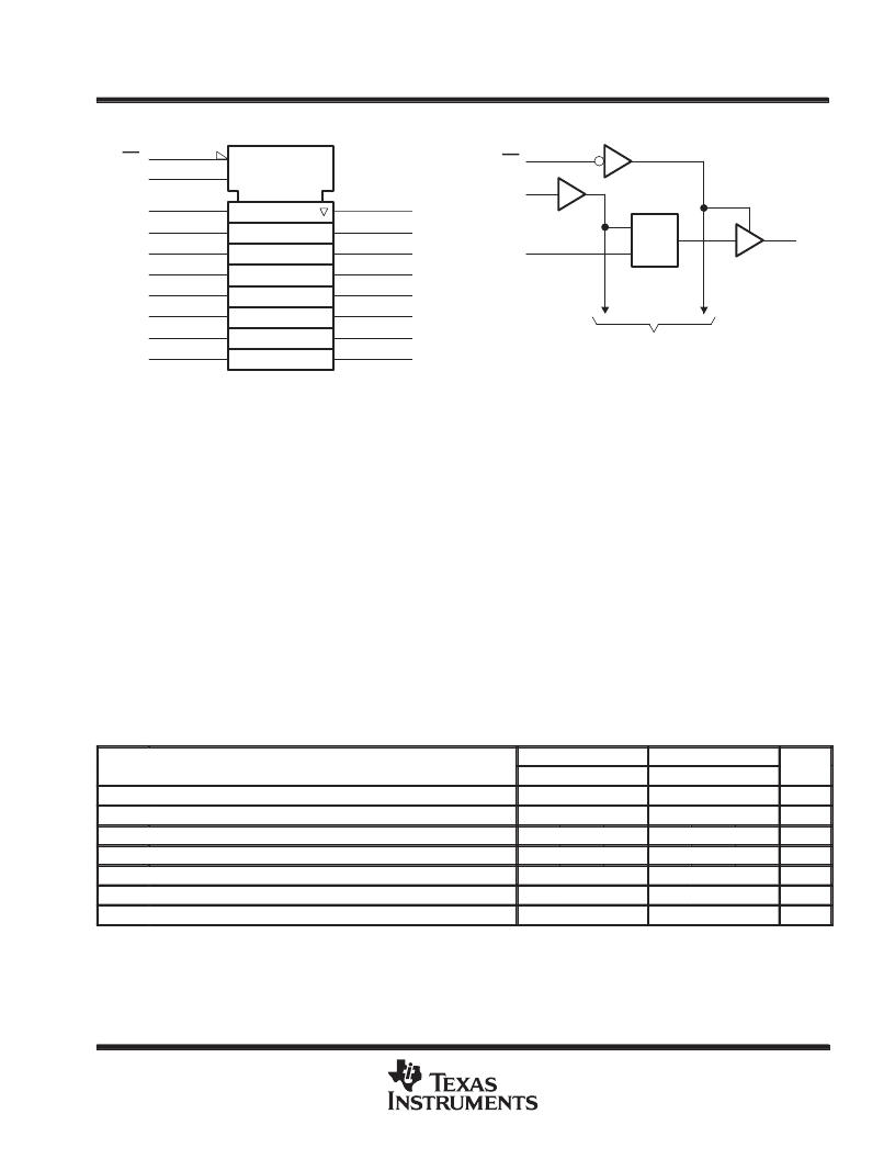
logic symbol
logic diagram (positive logic)
OE
LE
1D
2
1D
3
2D
4
3D
5
4D
6
5D
C1
11
1Q
19
2Q
18
3Q
17
4Q
16
5Q
15
6Q
14
7Q
13
8Q
12
7
6D
8
7D
9
8D
EN
1
OE
LE
1D
1Q
1
11
2
19
To Seven Other Channels
C1
1D
This symbol is in accordance with ANSI/IEEE Std 91-1984
and IEC Publication 617-12.
absolute maximum ratings over operating free-air temperature range (unless otherwise noted)
Supply voltage range, V
CC
Input voltage range, V
I
(see Note 1)
Voltage range applied to any output in the disabled or power-off state, V
O
Voltage range applied to any output in the high state, V
O
Input clamp current, I
IK
(V
I
< 0)
. . . . . . . . . . . . . . . . . . . . . . . . . . . . . . . . . . . . . . . . . . . . . . . . . . . . . . . . . .
Current into any output in the low state, I
O
: SN54BCT573
SN74BCT573
Operating free-air temperature range:
SN54BCT573
SN74BCT573
Storage temperature range
. . . . . . . . . . . . . . . . . . . . . . . . . . . . . . . . . . . . . . . . . . . . . . . . . . . . . . . .
– 0.5 V to 7 V
– 0.5 V to 7 V
– 0.5 V to 5.5 V
– 0.5 V to V
CC
–30 mA
. . . . . . . . . . . . . . . . . . . . . . . . . . . . . . . . . . . . . . . . . . . . . . . . . . . . . . . . . .
. . . . . . . . . . . . . . . . . . . . . . . . . . . . . . . . . . . . . . . . . . . . . . . . . . .
. . . . . . . . . . . . . . .
. . . . . . . . . . . . . . . . . . . . . . . . . . . . . . .
96 mA
128 mA
. . . . . . . . . . . . . . . . . . . . . . . . . . . . . . . . . . . . .
. . . . . . . . . . . . . . . . . . . . . . . . . . . . . . . . . . . .
. . . . . . . . . . . . . . . . . . . . . . . . . . . . .
. . . . . . . . . . . . . . . . . . . . . . . . . . . . . . . . .
– 55
°
C to 125
°
C
0
°
C to 70
°
C
– 65
°
C to 150
°
C
Stresses beyond those listed under “absolute maximum ratings” may cause permanent damage to the device. These are stress ratings only, and
functional operation of the device at these or any other conditions beyond those indicated under “recommended operating conditions” is not
implied. Exposure to absolute-maximum-rated conditions for extended periods may affect device reliability.
NOTE 1: The input and output negative-voltage ratings may be exceeded if the input and output clamp-current ratings are observed.
recommended operating conditions
SN54BCT573
MIN
NOM
SN74BCT573
MIN
NOM
UNIT
MAX
MAX
VCC
VIH
VIL
IIK
IOH
IOL
TA
Supply voltage
4.5
5
5.5
4.5
5
5.5
V
High-level input voltage
2
2
V
Low-level input voltage
0.8
0.8
V
Input clamp current
–18
–18
mA
High-level output current
–12
–15
mA
Low-level output current
48
64
mA
°
C
Operating free-air temperature
–55
125
0
70
相關(guān)PDF資料 |
PDF描述 |
|---|---|
| SN54BCT574FK | OCTAL EDGE-TRIGGERED D-TYPE FLIP-FLOPS WITH 3-STATE OUTPUTS |
| SN54BCT574J | OCTAL EDGE-TRIGGERED D-TYPE FLIP-FLOPS WITH 3-STATE OUTPUTS |
| SN54BCT574W | OCTAL EDGE-TRIGGERED D-TYPE FLIP-FLOPS WITH 3-STATE OUTPUTS |
| SN54CBT16244WD | 16-BIT FET BUS SWITCHES |
| SN74CBT16244DGG | 16-BIT FET BUS SWITCHES |
相關(guān)代理商/技術(shù)參數(shù) |
參數(shù)描述 |
|---|---|
| SN54BCT623W | 制造商:Texas Instruments 功能描述: |
| SN54BCT760J | 制造商:Texas Instruments 功能描述:Buffer/Line Driver 8-CH Non-Inverting 3-ST/Open Collector BiCMOS 20-Pin CDIP Tube 制造商:Texas Instruments 功能描述:OCTAL BUS DRIVER |
| SN54F00J | 制造商:Texas Instruments 功能描述:NAND Gate 4-Element 2-IN Bipolar 14-Pin CDIP Tube 制造商:Rochester Electronics LLC 功能描述:- Bulk |
| SN54F02J | 制造商:Texas Instruments 功能描述:NOR Gate 4-Element 2-IN Bipolar 14-Pin CDIP Tube 制造商:Rochester Electronics LLC 功能描述:- Bulk |
| SN54F04J | 制造商:Texas Instruments 功能描述: 制造商:Texas Instruments 功能描述:HEX INVERTER - Rail/Tube 制造商:Texas Instruments 功能描述:Inverter 6-Element Bipolar 14-Pin CDIP Tube |
發(fā)布緊急采購,3分鐘左右您將得到回復(fù)。