- 您現(xiàn)在的位置:買賣IC網(wǎng) > PDF目錄374865 > SN54BCT245J (Texas Instruments, Inc.) Reference Voltage Generator for VCOM Adjustment 8-TSSOP PDF資料下載
參數(shù)資料
| 型號: | SN54BCT245J |
| 廠商: | Texas Instruments, Inc. |
| 英文描述: | Reference Voltage Generator for VCOM Adjustment 8-TSSOP |
| 中文描述: | 八路總線收發(fā)器與三態(tài)輸出 |
| 文件頁數(shù): | 2/7頁 |
| 文件大小: | 102K |
| 代理商: | SN54BCT245J |
SN54BCT245, SN74BCT245
OCTAL BUS TRANSCEIVERS
WITH 3-STATE OUTPUTS
SCBS013F – SEPTEMBER 1988 – REVISED APRIL 1994
2–2
POST OFFICE BOX 655303
DALLAS, TEXAS 75265
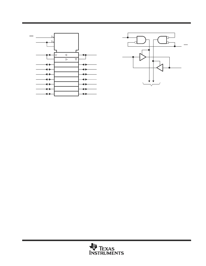
logic symbol
logic diagram (positive logic)
A5
6
A6
7
A7
8
A8
9
A2
3
A3
4
A4
5
OE
A1
2
G3
19
3EN2[AB]
B5
14
B6
13
B7
12
B8
11
B1
18
B2
17
B3
16
B4
15
3EN1[BA]
1
DIR
DIR
OE
A1
B1
1
2
18
19
To Seven Other Channels
1
2
This symbol is in accordance with ANSI/IEEE Std 91-1984
and IEC Publication 617-12.
absolute maximum ratings over operating free-air temperature range (unless otherwise noted)
Supply voltage range, V
CC
Input voltage range: Control inputs (see Note 1)
I/O ports (see Note 1)
Voltage range applied to any output in the disabled or power-off state, V
O
Voltage range applied to any output in the high state, V
O
Current into any output in the low state: SN54BCT245
– 0.5 V to 7 V
– 0.5 V to 7 V
– 0.5 V to 5.5 V
– 0.5 V to 7 V
– 0.5 V to V
CC
. . . . . . . . . . . . . . . . . . . . . . . . . . . . . . . . . . . . . . . . . . . . . . . . . . . . . . . . . .
. . . . . . . . . . . . . . . . . . . . . . . . . . . . . . . . . . . . . . . .
. . . . . . . . . . . . . . . . . . . . . . . . . . . . . . . . . . . . . . . . . .
. . . . . . . . . . . . . . . . .
. . . . . . . . . . . . . . . . . . . . . . . . . . . . . . .
. . . . . . . . . . . . . . . . . . . . . . . . . . . . . . . . . . . . . . . .
. . . . . . . . . . . . . . . . . . . . . . . . . . . . . . . . . . . . . . .
. . . . . . . . . . . . . . . . . . . . . . . . . . . . . . . . . . . . . . . . . .
SN54BCT245
. . . . . . . . . . . . . . . . . . . . . . . . . . . . . . . .
SN74BCT245
. . . . . . . . . . . . . . . . . . . . . . . . . . . . . . . . . . . .
. . . . . . . . . . . . . . . . . . . . . . . . . . . . . . . . . . . . . . . . . . . . . . . . . . . . . . . .
96 mA
128 mA
650 mW
SN74BCT245
Power dissipation (DB package only) (see Note 2)
Operating free-air temperature range:
– 55
°
C to 125
°
C
0
°
C to 70
°
C
– 65
°
C to 150
°
C
Storage temperature range
Stresses beyond those listed under “absolute maximum ratings” may cause permanent damage to the device. These are stress ratings only, and
functional operation of the device at these or any other conditions beyond those indicated under “recommended operating conditions” is not
implied. Exposure to absolute-maximum-rated conditions for extended periods may affect device reliability.
NOTES:
1. The input and output voltage ratings may be exceeded if the input and output current ratings are observed.
2. Power dissipation is application dependent and is a function of supply voltage, operating temperature, the number of outputs
switching simultaneously, and output duty cycle. Because the thermal resistance of the DB package is higher than that of the DW
or N packages, the DB package may not be suitable for some applications.
相關(guān)PDF資料 |
PDF描述 |
|---|---|
| SN54BCT245W | Reference Voltage Generator for VCOM Adjustment 8-TSSOP |
| SN74BCT543DWR | OCTAL REGISTERED TRANSCEIVERS WITH 3-STATE OUTPUTS |
| SN74CB3Q16245DGG | 16-BIT SWITCH 2.5-V/3.3-V LOW-VOLTAGE FET BUS SWITCH |
| SN74CBT16210CDGG | 20-BIT FET BUS SWITCH 5-V BUS SWITCH WITH -2-V UNDERSHOOT PROTECTION |
| SN74CBT16211ADGG | Single 2 Input NAND Gate, Open Drain; Package: SC-88A, SOT-353, SC-70 5 LEAD; No of Pins: 5; Container: Tape and Reel; Qty per Container: 3000 |
相關(guān)代理商/技術(shù)參數(shù) |
參數(shù)描述 |
|---|---|
| SN54BCT623W | 制造商:Texas Instruments 功能描述: |
| SN54BCT760J | 制造商:Texas Instruments 功能描述:Buffer/Line Driver 8-CH Non-Inverting 3-ST/Open Collector BiCMOS 20-Pin CDIP Tube 制造商:Texas Instruments 功能描述:OCTAL BUS DRIVER |
| SN54F00J | 制造商:Texas Instruments 功能描述:NAND Gate 4-Element 2-IN Bipolar 14-Pin CDIP Tube 制造商:Rochester Electronics LLC 功能描述:- Bulk |
| SN54F02J | 制造商:Texas Instruments 功能描述:NOR Gate 4-Element 2-IN Bipolar 14-Pin CDIP Tube 制造商:Rochester Electronics LLC 功能描述:- Bulk |
| SN54F04J | 制造商:Texas Instruments 功能描述: 制造商:Texas Instruments 功能描述:HEX INVERTER - Rail/Tube 制造商:Texas Instruments 功能描述:Inverter 6-Element Bipolar 14-Pin CDIP Tube |
發(fā)布緊急采購,3分鐘左右您將得到回復(fù)。