- 您現(xiàn)在的位置:買賣IC網(wǎng) > PDF目錄374851 > SN54AS651FK (Texas Instruments, Inc.) OCTAL BUS TRANSCEIVERS AND REGISTERS WITH 3-STATE OUTPUTS PDF資料下載
參數(shù)資料
| 型號: | SN54AS651FK |
| 廠商: | Texas Instruments, Inc. |
| 英文描述: | OCTAL BUS TRANSCEIVERS AND REGISTERS WITH 3-STATE OUTPUTS |
| 中文描述: | 八路總線收發(fā)器和寄存器具有三態(tài)輸出 |
| 文件頁數(shù): | 7/22頁 |
| 文件大?。?/td> | 331K |
| 代理商: | SN54AS651FK |
SN54ALS652, SN54ALS653, SN54AS651, SN54AS652
SN74ALS651A, SN74ALS652A, SN74ALS653, SN74ALS654, SN74AS651, SN74AS652
OCTAL BUS TRANSCEIVERS AND REGISTERS WITH 3-STATE OUTPUTS
SDAS066F – DECEMBER 1983 – REVISED OCTOBER 1996
7
POST OFFICE BOX 655303
DALLAS, TEXAS 75265
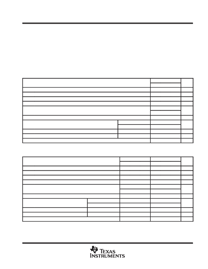
absolute maximum ratings over operating free-air temperature range (unless otherwise noted)
Supply voltage, V
CC
Input voltage, V
I
: Control inputs
7 V
7 V
5.5 V
. . . . . . . . . . . . . . . . . . . . . . . . . . . . . . . . . . . . . . . . . . . . . . . . . . . . . . . . . . . . . . . . . . . . . . .
. . . . . . . . . . . . . . . . . . . . . . . . . . . . . . . . . . . . . . . . . . . . . . . . . . . . . . . . . . . . . .
I/O ports
. . . . . . . . . . . . . . . . . . . . . . . . . . . . . . . . . . . . . . . . . . . . . . . . . . . . . . . . . . . . . . . . .
Operating free-air temperature range, T
A
: SN54ALS652
SN74ALS651A, SN74ALS652A
Storage temperature range, T
stg
. . . . . . . . . . . . . . . . . . . . . . . . . . . . . . . . . . . . . . . . . . . . . . . . . .
Stresses beyond those listed under “absolute maximum ratings” may cause permanent damage to the device. These are stress ratings only, and
functional operation of the device at these or any other conditions beyond those indicated under “recommended operating conditions” is not
implied. Exposure to absolute-maximum-rated conditions for extended periods may affect device reliability.
–55
°
C to 125
°
C
0
°
C to 70
°
C
–65
°
C to 150
°
C
. . . . . . . . . . . . . . . . . . . . . . . . . . . . . .
. . . . . . . . . . . . . . . . .
recommended operating conditions
SN74ALS651A
UNIT
MIN
NOM
MAX
VCC
VIH
VIL
IOH
Supply voltage
4.5
5
5.5
V
High-level input voltage
2
V
Low-level input voltage
0.8
V
High-level output current
–15
mA
IOL
Low level output current
Low-level output current
24
48
40
mA
fclock
Clock frequency
0
MHz
tw
Pulse duration
CLKBA or CLKAB high
12.5
ns
CLKBA or CLKAB low
12.5
tsu
th
TA
Applies only to the SN74ALS651A-1 and only if VCC is maintained between 4.75 V and 5.25 V
Setup time before CLKAB
↑
or CLKBA
↑
Hold time after CLKAB
↑
or CLKBA
↑
Operating free-air temperature
A or B
10
ns
A or B
0
ns
°
C
0
70
recommended operating conditions
SN54ALS652
MIN
NOM
SN74ALS652A
MIN
NOM
UNIT
MAX
MAX
VCC
VIH
VIL
IOH
Supply voltage
4.5
5
5.5
4.5
5
5.5
V
High-level input voltage
2
2
V
Low-level input voltage
0.7
0.8
V
High-level output current
–12
–15
mA
IOL
Low level output current
Low-level output current
12
24
48
mA
fclock
Clock frequency
0
35
0
40
MHz
tw
Pulse duration
CLKBA or CLKAB high
14.5
12.5
ns
CLKBA or CLKAB low
14.5
12.5
tsu
th
TA
Applies only to the SN74ALS652A-1 and only if VCC is maintained between 4.75 V and 5.25 V
Setup time before CLKAB
↑
or CLKBA
↑
Hold time after CLKAB
↑
or CLKBA
↑
Operating free-air temperature
A or B
15
10
ns
A or B
5
0
ns
°
C
–55
125
0
70
相關PDF資料 |
PDF描述 |
|---|---|
| SN54AS652FK | OCTAL BUS TRANSCEIVERS AND REGISTERS WITH 3-STATE OUTPUTS |
| SN54ALS652FK | OCTAL BUS TRANSCEIVERS AND REGISTERS WITH 3-STATE OUTPUTS |
| SN54ALS653FK | OCTAL BUS TRANSCEIVERS AND REGISTERS WITH 3-STATE OUTPUTS |
| SN54ALS653JT | OCTAL BUS TRANSCEIVERS AND REGISTERS WITH 3-STATE OUTPUTS |
| SN54AS804BFK | HEX 2-INPUT NAND DRIVERS |
相關代理商/技術參數(shù) |
參數(shù)描述 |
|---|---|
| SN54AS652JT | 制造商:Texas Instruments 功能描述:Bus XCVR Single 8-CH 3-ST 24-Pin CDIP Tube |
| SN54AS74AJ | 制造商:Texas Instruments 功能描述:Flip Flop D-Type Pos-Edge 2-Element 14-Pin CDIP Tube 制造商:Rochester Electronics LLC 功能描述:- Bulk 制造商:Texas Instruments 功能描述:FLIP FLOP D-TYPE POS-EDGE 2-ELEM 14CDIP - Rail/Tube |
| SN54AS74FK | 制造商:Texas Instruments 功能描述: |
| SN54AS756J | 制造商:Texas Instruments 功能描述:Buffer/Line Driver 8-CH Inverting 3-ST/Open Collector Bipolar 20-Pin CDIP Tube 制造商:Texas Instruments 功能描述:BFFR/LINE DRVR 8CH INV 3-ST/OPEN COLLECTOR BIPOLAR 20CDIP - Rail/Tube |
| SN54AS760J | 制造商:Texas Instruments 功能描述: |
發(fā)布緊急采購,3分鐘左右您將得到回復。