- 您現(xiàn)在的位置:買賣IC網(wǎng) > PDF目錄374861 > SN54ACT373J (Texas Instruments, Inc.) OCTAL D-TYPE TRANSPARENT LATCHES WITH 3-STATE OUTPUTS PDF資料下載
參數(shù)資料
| 型號: | SN54ACT373J |
| 廠商: | Texas Instruments, Inc. |
| 英文描述: | OCTAL D-TYPE TRANSPARENT LATCHES WITH 3-STATE OUTPUTS |
| 中文描述: | 八路?- 3型透明鎖存態(tài)輸出 |
| 文件頁數(shù): | 2/6頁 |
| 文件大?。?/td> | 83K |
| 代理商: | SN54ACT373J |
SN54ACT373, SN74ACT373
OCTAL D-TYPE TRANSPARENT LATCHES
WITH 3-STATE OUTPUTS
SCAS544D – OCTOBER 1995 – REVISED JANUARY 2000
2
POST OFFICE BOX 655303
DALLAS, TEXAS 75265
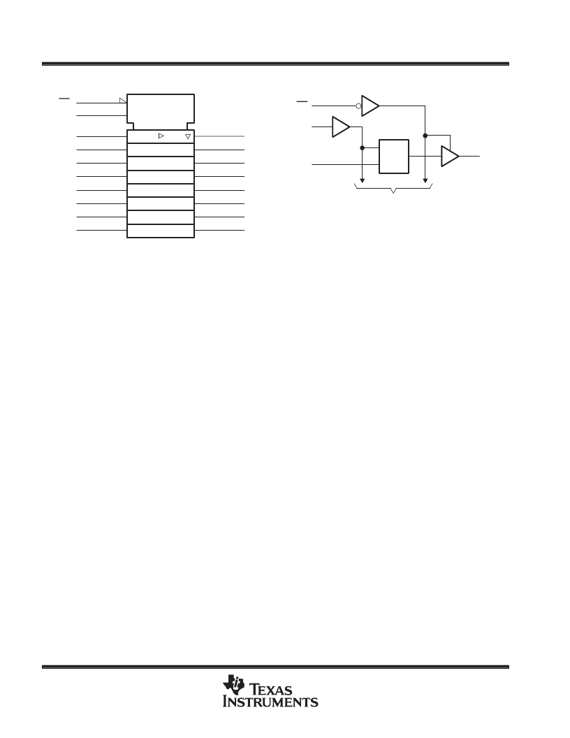
logic symbol
This symbol is in accordance with ANSI/IEEE Std 91-1984 and
IEC Publication 617-12.
OE
LE
1D
3
1D
4
2D
7
3D
8
4D
13
5D
C1
11
1Q
2
2Q
5
3Q
6
4Q
9
5Q
12
6Q
15
7Q
16
8Q
19
14
6D
17
7D
18
8D
EN
1
logic diagram (positive logic)
OE
LE
1D
1Q
To Seven Other Channels
C1
1D
1
11
3
2
absolute maximum ratings over operating free-air temperature range (unless otherwise noted)
Supply voltage range, V
CC
Input voltage range, V
I
(see Note 1)
Output voltage range, V
O
(see Note 1)
Input clamp current, I
IK
(V
I
< 0 or V
I
> V
CC)
Output clamp current, I
OK
(V
O
< 0 or V
O
> V
CC)
Continuous output current, I
O
(V
O
= 0 to V
CC
)
Continuous current through V
CC
or GND
Package thermal impedance,
θ
JA
(see Note 2): DB package
–0.5 V to 7 V
. . . . . . . . . . . . . . . . . . . . . . . . . . . . . . . . . . . . . . . . . . . . . . . . . . . . . . . . . .
. . . . . . . . . . . . . . . . . . . . . . . . . . . . . . . . . . . . . . . . . . .
. . . . . . . . . . . . . . . . . . . . . . . . . . . . . . . . . . . . . . . .
. . . . . . . . . . . . . . . . . . . . . . . . . . . . . . . . . . . . . . . . . . . . . . . .
. . . . . . . . . . . . . . . . . . . . . . . . . . . . . . . . . . . . . . . . . . . .
. . . . . . . . . . . . . . . . . . . . . . . . . . . . . . . . . . . . . . . . . . . . . .
. . . . . . . . . . . . . . . . . . . . . . . . . . . . . . . . . . . . . . . . . . . . . . . . . .
. . . . . . . . . . . . . . . . . . . . . . . . . . . . . . . . .
DW package
. . . . . . . . . . . . . . . . . . . . . . . . . . . . . . . . .
N package
. . . . . . . . . . . . . . . . . . . . . . . . . . . . . . . . . . .
PW package
. . . . . . . . . . . . . . . . . . . . . . . . . . . . . . . . .
Storage temperature range, T
stg
. . . . . . . . . . . . . . . . . . . . . . . . . . . . . . . . . . . . . . . . . . . . . . . . . . .
–0.5 V to V
CC
+ 0.5 V
–0.5 V to V
CC
+ 0.5 V
±
20 mA
±
20 mA
±
50 mA
±
200 mA
70
°
C/W
58
°
C/W
69
°
C/W
83
°
C/W
–65
°
C to 150
°
C
Stresses beyond those listed under “absolute maximum ratings” may cause permanent damage to the device. These are stress ratings only, and
functional operation of the device at these or any other conditions beyond those indicated under “recommended operating conditions” is not
implied. Exposure to absolute-maximum-rated conditions for extended periods may affect device reliability.
NOTES:
1. The input and output voltage ratings may be exceeded if the input and output current ratings are observed.
2. The package thermal impedance is calculated in accordance with JESD 51.
相關PDF資料 |
PDF描述 |
|---|---|
| SN54ACT373W | OCTAL D-TYPE TRANSPARENT LATCHES WITH 3-STATE OUTPUTS |
| SN74ACT374DB | OCTAL D-TYPE EDGE-TRIGGERED FLIP-FLOPS WITH 3-STATE OUTPUTS |
| SN54ACT374FK | OCTAL D-TYPE EDGE-TRIGGERED FLIP-FLOPS WITH 3-STATE OUTPUTS |
| SN54ACT374J | OCTAL D-TYPE EDGE-TRIGGERED FLIP-FLOPS WITH 3-STATE OUTPUTS |
| SN54ACT374W | OCTAL D-TYPE EDGE-TRIGGERED FLIP-FLOPS WITH 3-STATE OUTPUTS |
相關代理商/技術參數(shù) |
參數(shù)描述 |
|---|---|
| SN54ACT373W | 制造商:TI 制造商全稱:Texas Instruments 功能描述:OCTAL D-TYPE TRANSPARENT LATCHES WITH 3-STATE OUTPUTS |
| SN54ACT374 | 制造商:TI 制造商全稱:Texas Instruments 功能描述:OCTAL D-TYPE EDGE-TRIGGERED FLIP-FLOPS WITH 3-STATE OUTPUTS |
| SN54ACT374_02 | 制造商:TI 制造商全稱:Texas Instruments 功能描述:OCTAL D-TYPE EDGE-TRIGGERED FLIP-FLOPS WITH 3-STATE OUTPUTS |
| SN54ACT374_08 | 制造商:TI 制造商全稱:Texas Instruments 功能描述:OCTAL D-TYPE EDGE-TRIGGERED FLIP-FLOPS WITH 3-STATE OUTPUTS |
| SN54ACT374FK | 制造商:TI 制造商全稱:Texas Instruments 功能描述:OCTAL D-TYPE EDGE-TRIGGERED FLIP-FLOPS WITH 3-STATE OUTPUTS |
發(fā)布緊急采購,3分鐘左右您將得到回復。