- 您現(xiàn)在的位置:買賣IC網(wǎng) > PDF目錄374848 > SN54ACT16245WD (Texas Instruments, Inc.) 16-BIT BUS TRANSCEIVERS WITH 3-STATE OUTPUTS PDF資料下載
參數(shù)資料
| 型號: | SN54ACT16245WD |
| 廠商: | Texas Instruments, Inc. |
| 元件分類: | 通用總線功能 |
| 英文描述: | 16-BIT BUS TRANSCEIVERS WITH 3-STATE OUTPUTS |
| 中文描述: | 16位總線收發(fā)3態(tài)輸出 |
| 文件頁數(shù): | 3/6頁 |
| 文件大?。?/td> | 100K |
| 代理商: | SN54ACT16245WD |
SN54ACT16245, 74ACT16245
16-BIT BUS TRANSCEIVERS
WITH 3-STATE OUTPUTS
SCAS097B – DECEMBER 1989 – REVISED APRIL 1996
3
POST OFFICE BOX 655303
DALLAS, TEXAS 75265
absolute maximum ratings over operating free-air temperature range (unless otherwise noted)
Supply voltage, V
CC
Input voltage range, V
I
(see Note 1)
Output voltage range, V
O
(see Note 1)
Input clamp current, I
IK
(V
I
< 0 or V
I
> V
CC
)
Output clamp current, I
OK
(V
O
< 0 or V
O
> V
CC
)
Continuous output current, I
O
(V
O
= 0 to V
CC
)
Continuous current through V
CC
or GND
Maximum power dissipation at T
A
= 55
°
C (in still air) (see Note 2):DGG package
–0.5 V to 7 V
. . . . . . . . . . . . . . . . . . . . . . . . . . . . . . . . . . . . . . . . . . . . . . . . . . . . . . . . . . . . . . . .
. . . . . . . . . . . . . . . . . . . . . . . . . . . . . . . . . . . . . . . . . . . .
. . . . . . . . . . . . . . . . . . . . . . . . . . . . . . . . . . . . . . . . .
. . . . . . . . . . . . . . . . . . . . . . . . . . . . . . . . . . . . . . . . . . . . . . . . .
. . . . . . . . . . . . . . . . . . . . . . . . . . . . . . . . . . . . . . . . . . . .
. . . . . . . . . . . . . . . . . . . . . . . . . . . . . . . . . . . . . . . . . . . . . .
. . . . . . . . . . . . . . . . . . . . . . . . . . . . . . . . . . . . . . . . . . . . . . . . . .
–0.5 V to V
CC
+ 0.5 V
–0.5 V to V
CC
+ 0.5 V
±
20 mA
±
50 mA
±
50 mA
±
400 mA
0.85 W
1.2 W
. . . . . . . . . . . . . . . .
. . . . . . . . . . . . . . . . . . .
DL package
Storage temperature range, T
stg
Stresses beyond those listed under “absolute maximum ratings” may cause permanent damage to the device. These are stress ratings only, and
functional operation of the device at these or any other conditions beyond those indicated under “recommended operating conditions” is not
implied. Exposure to absolute-maximum-rated conditions for extended periods may affect device reliability.
NOTES:
1. The input and output voltage ratings may be exceeded if the input and output current ratings are observed.
2. The maximum package power dissipation is calculated using a junction temperature of 150 C and a board trace length of 750 mils.
–65
°
C to 150
°
C
. . . . . . . . . . . . . . . . . . . . . . . . . . . . . . . . . . . . . . . . . . . . . . . . . . . .
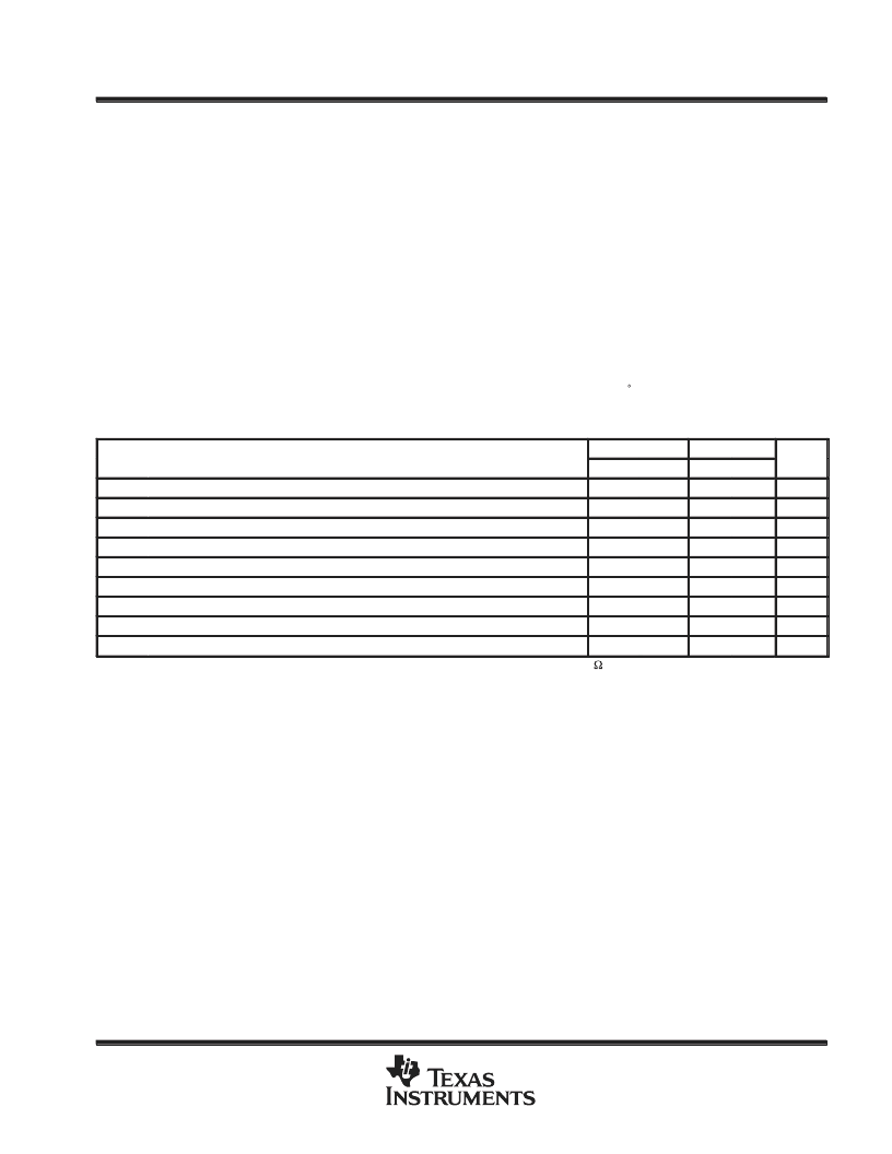
recommended operating conditions (see Note 3)
SN54ACT16245
MIN
74ACT16245
MIN
UNIT
MAX
MAX
VCC
VIH
VIL
VI
VO
IOH
IOL
t/
v
TA
NOTES:
Supply voltage (see Note 4)
4.5
5.5
4.5
5.5
V
High-level input voltage
2
2
V
Low-level input voltage
0.8
0.8
V
Input voltage
0
VCC
VCC
–24
0
VCC
VCC
–24
V
Output voltage
0
0
V
High-level output current
mA
Low-level output current
24
24
mA
Input transition rise or fall rate
0
10
0
10
ns/V
°
C
Operating free-air temperature
–55
125
–40
85
3. Unused inputs should be tied to VCC through a pullup resistor of approximately 5 k or greater to keep them from floating.
4. All VCC and GND pins must be connected to the proper voltage power supply.
相關(guān)PDF資料 |
PDF描述 |
|---|---|
| SN54ACT241FK | OCTAL BUFFERS/DRIVERS WITH 3-STATE OUTPUTS |
| SN54ACT241J | OCTAL BUFFERS/DRIVERS WITH 3-STATE OUTPUTS |
| SN54ACT241W | OCTAL BUFFERS/DRIVERS WITH 3-STATE OUTPUTS |
| SN74ACT241DB | Low-Voltage CMOS Octal Transceiver; Package: SOIC-20 WB; No of Pins: 20; Container: Rail; Qty per Container: 38 |
| SN54AH573 | OCTAL TRANSPARENT D-TYPE LATCHES WITH 3-STATE OUTPUTS |
相關(guān)代理商/技術(shù)參數(shù) |
參數(shù)描述 |
|---|---|
| SN54ACT16373 | 制造商:TI 制造商全稱:Texas Instruments 功能描述:16-BIT D-TYPE TRANSPARENT LATCHES WITH 3-STATE OUTPUTS |
| SN54ACT16373WD | 制造商:TI 制造商全稱:Texas Instruments 功能描述:16-BIT D-TYPE TRANSPARENT LATCHES WITH 3-STATE OUTPUTS |
| SN54ACT16374 | 制造商:TI 制造商全稱:Texas Instruments 功能描述:16-BIT D-TYPE EDGE-TRIGGERED FLIP-FLOPS WITH 3-STATE OUTPUTS |
| SN54ACT16374WD | 制造商:TI 制造商全稱:Texas Instruments 功能描述:16-BIT D-TYPE EDGE-TRIGGERED FLIP-FLOPS WITH 3-STATE OUTPUTS |
| SN54ACT16651 | 制造商:TI 制造商全稱:Texas Instruments 功能描述:16-BIT TRANSCEIVERS AND REGISTERS WITH 3-STATE OUTPUTS |
發(fā)布緊急采購,3分鐘左右您將得到回復(fù)。