- 您現(xiàn)在的位置:買(mǎi)賣(mài)IC網(wǎng) > PDF目錄374847 > SN54ABT8245JT (Texas Instruments, Inc.) SCAN TEST DEVICES WITH OCTAL BUS TRANSCEIVERS PDF資料下載
參數(shù)資料
| 型號(hào): | SN54ABT8245JT |
| 廠商: | Texas Instruments, Inc. |
| 英文描述: | SCAN TEST DEVICES WITH OCTAL BUS TRANSCEIVERS |
| 中文描述: | 掃描測(cè)試設(shè)備與八進(jìn)制總線收發(fā)器 |
| 文件頁(yè)數(shù): | 13/25頁(yè) |
| 文件大?。?/td> | 364K |
| 代理商: | SN54ABT8245JT |
第1頁(yè)第2頁(yè)第3頁(yè)第4頁(yè)第5頁(yè)第6頁(yè)第7頁(yè)第8頁(yè)第9頁(yè)第10頁(yè)第11頁(yè)第12頁(yè)當(dāng)前第13頁(yè)第14頁(yè)第15頁(yè)第16頁(yè)第17頁(yè)第18頁(yè)第19頁(yè)第20頁(yè)第21頁(yè)第22頁(yè)第23頁(yè)第24頁(yè)第25頁(yè)
SN54ABT8245, SN74ABT8245
SCAN TEST DEVICES
WITH OCTAL BUS TRANSCEIVERS
SCBS124D – AUGUST 1992 – REVISED DECEMBER 1996
13
POST OFFICE BOX 655303
DALLAS, TEXAS 75265
boundary-control-register opcode description
The BCR opcodes are decoded from BCR bits 2–0 as shown in Table 4. The selected test operation is
performed while the RUNT instruction is executed in the Run-Test/Idle state. The following descriptions detail
the operation of each BCR instruction and illustrate the associated PSA and PRPG algorithms.
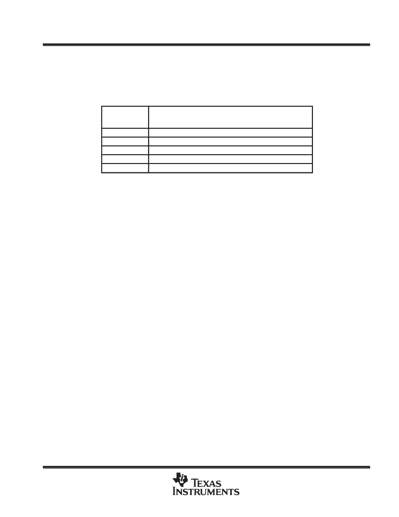
Table 4. Boundary-Control Register Opcodes
BINARY CODE
BIT 2
→
BIT 0
MSB
→
LSB
X00
DESCRIPTION
Sample inputs/toggle outputs (TOPSIP)
X01
Pseudo-random pattern generation/16-bit mode (PRPG)
X10
Parallel-signature analysis/16-bit mode (PSA)
011
Simultaneous PSA and PRPG/8-bit mode (PSA/PRPG)
111
Simultaneous PSA and binary count up/8-bit mode (PSA/COUNT)
It should be noted, in general, that while the control input BSCs (bits 35–32) are not included in the sample,
toggle, PSA, PRPG, or COUNT algorithms, the output-enable BSCs (bits 35–34 of the BSR) do control the drive
state (active or high impedance) of the selected device output pins. It also should be noted that these BCR
instructions are only valid when the device is operating in one direction of data flow (that is, OEA
≠
OEB).
Otherwise, the bypass instruction is operated.
PSA input masking
Bits 10–3 of the BCR specify device input pins to be masked from PSA operations. Bit 10 selects masking for
device input pin A8 during A-to-B data flow or for device input pin B8 during B-to-A data flow. Bit 3 selects
masking for device input pins A1 or B1 during A-to-B or B-to-A data flow, respectively. Bits intermediate to 10
and 3 mask corresponding device input pins, in order, from most significant to least significant, as indicated in
Table 3. When the mask bit that corresponds to a particular device input has a logic 1 value, the device input
pin is masked from any PSA operation, meaning that the state of the device input pin is ignored and has no effect
on the generated signature. Otherwise, when a mask bit has a logic 0 value, the corresponding device input
is not masked from the PSA operation.
sample inputs/toggle outputs (TOPSIP)
Data appearing at the selected device input pins is captured in the shift-register elements of the selected BSCs
on each rising edge of TCK. This data is updated in the shadow latches of the selected input BSCs and applied
to the inputs of the normal on-chip logic. Data in the shift-register elements of the selected output BSCs is
toggled on each rising edge of TCK, updated in the shadow latches, and applied to the associated device output
pins on each falling edge of TCK.
相關(guān)PDF資料 |
PDF描述 |
|---|---|
| SN54ABT827FK | 10-BIT BUFFERS/DRIVERS WITH 3-STATE OUTPUTS |
| SN54ABT827JT | 10-BIT BUFFERS/DRIVERS WITH 3-STATE OUTPUTS |
| SN74ABT827DB | 10-BIT BUFFERS/DRIVERS WITH 3-STATE OUTPUTS |
| SN54ABT833 | 8-BIT TO 9-BIT PARITY BUS TRANSCEIVERS |
| SN54ABT833FK | 8-BIT TO 9-BIT PARITY BUS TRANSCEIVERS |
相關(guān)代理商/技術(shù)參數(shù) |
參數(shù)描述 |
|---|---|
| SN54ABT827 | 制造商:TI 制造商全稱:Texas Instruments 功能描述:10-BIT BUFFERS/DRIVERS WITH 3-STATE OUTPUTS |
| SN54ABT827FK | 制造商:TI 制造商全稱:Texas Instruments 功能描述:10-BIT BUFFERS/DRIVERS WITH 3-STATE OUTPUTS |
| SN54ABT827JT | 制造商:TI 制造商全稱:Texas Instruments 功能描述:10-BIT BUFFERS/DRIVERS WITH 3-STATE OUTPUTS |
| SN54ABT833 | 制造商:TI 制造商全稱:Texas Instruments 功能描述:8-BIT TO 9-BIT PARITY BUS TRANSCEIVERS |
| SN54ABT833FK | 制造商:TI 制造商全稱:Texas Instruments 功能描述:8-BIT TO 9-BIT PARITY BUS TRANSCEIVERS |
發(fā)布緊急采購(gòu),3分鐘左右您將得到回復(fù)。