- 您現(xiàn)在的位置:買(mǎi)賣(mài)IC網(wǎng) > PDF目錄374843 > SMJ416160 (Texas Instruments, Inc.) 1048576 BY 16-BIT DYNAMIC RANDOM-ACCESS MEMORIES PDF資料下載
參數(shù)資料
| 型號(hào): | SMJ416160 |
| 廠商: | Texas Instruments, Inc. |
| 英文描述: | 1048576 BY 16-BIT DYNAMIC RANDOM-ACCESS MEMORIES |
| 中文描述: | 1048576由16位動(dòng)態(tài)隨機(jī)存取存儲(chǔ)器 |
| 文件頁(yè)數(shù): | 8/24頁(yè) |
| 文件大小: | 356K |
| 代理商: | SMJ416160 |
第1頁(yè)第2頁(yè)第3頁(yè)第4頁(yè)第5頁(yè)第6頁(yè)第7頁(yè)當(dāng)前第8頁(yè)第9頁(yè)第10頁(yè)第11頁(yè)第12頁(yè)第13頁(yè)第14頁(yè)第15頁(yè)第16頁(yè)第17頁(yè)第18頁(yè)第19頁(yè)第20頁(yè)第21頁(yè)第22頁(yè)第23頁(yè)第24頁(yè)
SMJ416160, SMJ418160
1048576 BY 16-BIT
DYNAMIC RANDOM-ACCESS MEMORIES
SGMS720D – APRIL 1995 – REVISED SEPTEMBER 1997
8
POST OFFICE BOX 1443
HOUSTON, TEXAS 77251–1443
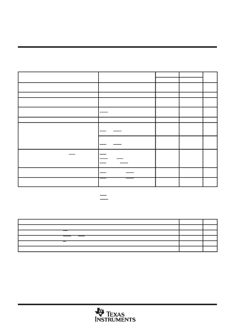
electrical characteristics over recommended ranges of supply voltage and operating free-air
temperature (unless otherwise noted) (continued)
SMJ418160
PARAMETER
TEST CONDITIONS
’418160-70
MIN
’418160-80
MIN
UNIT
MAX
MAX
VOH
High-level output
voltage
IOH = – 5 mA
2.4
2.4
V
VOL
Low-level output voltage
IOL = 4.2 mA
VCC = 5.5 V,
All others = 0 V to VCC
VCC = 5.5 V,
xCAS high
0.4
0.4
V
II
Input current (leakage)
VI = 0 V to 6.5 V,
±
10
±
10
μ
A
IO
Output current (leakage)
VO = 0 V to VCC,
±
10
±
10
μ
A
ICC1§
Read- or write-cycle current
VCC = 5.5 V,
VIH = 2.4 V (TTL),
After one memory cycle,
RAS and xCAS high
Minimum cycle
180
170
mA
ICC2
Standby current
2
2
mA
VIH = VCC – 0.2 V (CMOS),
After one memory cycle,
RAS and xCAS high
1
1
mA
ICC3§
Average refresh current (RAS only refresh or
CBR)
VCC = 5.5 V,
RAS cycling,
xCAS high (RAS only),
RAS low after xCAS low (CBR)
VCC = 5.5 V,
RAS low,
Minimum cycle,
180
170
mA
ICC4
Average page current
tPC = MIN,
xCAS cycling
180
170
mA
ICC7
Standby current, outputs enabled
RAS = VIH,
Data out = enabled
xCAS = VIL,
5
5
mA
For conditions shown as MIN/MAX, use the appropriate value specified in the timing requirements.
Measured with outputs open
§Measured with a maximum of one address change while RAS = VIL
Measured with a maximum of one address change while xCAS = VIH
capacitance over recommended ranges of supply voltage and operating free-air temperature,
f = 1 MHz (see Note 3)
PARAMETER
MIN
MAX
UNIT
pF
Ci(A)
Ci(OE)
Ci(RC)
Ci(W)
Co
#A10 and A11 are NC for SMJ418160.
NOTE 3: Capacitance is sampled only at initial design and after any major changes. Samples are tested at 0 V and 25
°
C with a 1-MHz signal
applied to the pin under test. All other pins are open.
Input capacitance, A0–A11#
8
Input capacitance, OE
8
pF
Input capacitance, xCAS and RAS
8
pF
Input capacitance, W
8
pF
Output capacitance
10
pF
相關(guān)PDF資料 |
PDF描述 |
|---|---|
| SMJ418160 | 1048576 BY 16-BIT DYNAMIC RANDOM-ACCESS MEMORIES |
| SMJ44C251 | 262144 BY 4-BIT MULTIPORT VIDEO RAM |
| SMJ44C256 | 262144 BY 4-BIT DYNAMIC RANDOM-ACCESS MEMORY |
| SMJ55161 | 262144 BY 16-BIT MULTIPORT VIDEO RAM |
| SMJ55166 | 262144 BY 16-BIT MULTIPORT VIDEO RAM |
相關(guān)代理商/技術(shù)參數(shù) |
參數(shù)描述 |
|---|---|
| SMJ416400 | 制造商:TI 制造商全稱:Texas Instruments 功能描述:4194304 BY 4-BIT DYNAMIC RANDOM-ACCESS MEMORY |
| SMJ4164-12FGE | 制造商:未知廠家 制造商全稱:未知廠家 功能描述:x1 Page Mode DRAM |
| SMJ4164-12FGS | 制造商:Rochester Electronics LLC 功能描述:- Bulk |
| SMJ4164-12JDE | 制造商:未知廠家 制造商全稱:未知廠家 功能描述:x1 Page Mode DRAM |
| SMJ4164-15FGE | 制造商:未知廠家 制造商全稱:未知廠家 功能描述:x1 Page Mode DRAM |
發(fā)布緊急采購(gòu),3分鐘左右您將得到回復(fù)。