- 您現(xiàn)在的位置:買賣IC網(wǎng) > PDF目錄374843 > SMJ320C6201BGLE (Texas Instruments, Inc.) DIGITAL SIGNAL PROCESSORS PDF資料下載
參數(shù)資料
| 型號: | SMJ320C6201BGLE |
| 廠商: | Texas Instruments, Inc. |
| 元件分類: | 數(shù)字信號處理 |
| 英文描述: | DIGITAL SIGNAL PROCESSORS |
| 中文描述: | 數(shù)字信號處理器 |
| 文件頁數(shù): | 2/73頁 |
| 文件大小: | 1093K |
| 代理商: | SMJ320C6201BGLE |
第1頁當前第2頁第3頁第4頁第5頁第6頁第7頁第8頁第9頁第10頁第11頁第12頁第13頁第14頁第15頁第16頁第17頁第18頁第19頁第20頁第21頁第22頁第23頁第24頁第25頁第26頁第27頁第28頁第29頁第30頁第31頁第32頁第33頁第34頁第35頁第36頁第37頁第38頁第39頁第40頁第41頁第42頁第43頁第44頁第45頁第46頁第47頁第48頁第49頁第50頁第51頁第52頁第53頁第54頁第55頁第56頁第57頁第58頁第59頁第60頁第61頁第62頁第63頁第64頁第65頁第66頁第67頁第68頁第69頁第70頁第71頁第72頁第73頁
SM320C6201, SMJ320C6201B
DIGITAL SIGNAL PROCESSORS
SGUS028A – NOVEMBER 1998 – REVISED JANUARY 1999
2
POST OFFICE BOX 1443
HOUSTON, TEXAS 77251–1443
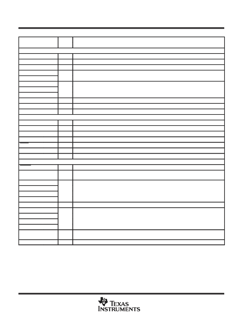
Signal Descriptions
SIGNAL
TYPE
DESCRIPTION
NAME
NO.
CLOCK/PLL
CLKIN
A14
I
Clock Input
CLKOUT1
Y6
O
Clock output at full device speed
CLKOUT2
V9
O
Clock output at half of device speed
CLKMODE1
B17
I
Clock mode select
Selects whether the output clock frequency = input clock freq x4 or x1
PLL frequency range (3, 2, and 1)
Selects one of three frequency ranges bounding the CLKOUT1 signal.
CLKOUT1 frequency determines the 3-bit value for the PLLFREQ pins.
PLL analog VCC connection for the low-pass filter
PLL analog GND connection for the low-pass filter
CLKMODE0
C17
PLLFREQ3
C13
PLLFREQ2
G11
I
PLLFREQ1
PLLV
PLLG
F11
D12
A§
A§
A§
G10
PLLF
C12
PLL low-pass filter connection to external components and a bypass capacitor
JTAG EMULATION
TMS
K19
I
JTAG test port mode select (features an internal pull-up)
TDO
R12
O/Z
JTAG test port data out
TDI
R13
I
JTAG test port data in (features an internal pull-up)
TCK
M20
I
JTAG test port clock
TRST
N18
I
JTAG test port reset (features an internal pull-down)
Emulation pin 1, pull-up with a dedicated 20-k
resistor
Emulation pin 0, pull-up with a dedicated 20-k
resistor
CONTROL
EMU1
R20
I/O/Z
EMU0
T18
I/O/Z
RESET
J20
I
Device reset
NMI
K21
I
Nonmaskable interrupt
Edge-driven (rising edge)
EXT_INT7
R16
EXT_INT6
P20
I
External interrupts
Edge-driven (rising edge)
EXT_INT5
R15
EXT_INT4
R18
IACK
R11
O
Interrupt acknowledge for all active interrupts serviced by the CPU
INUM3
T19
INUM2
T20
O
Active interrupt identification number
Valid during IACK for all active interrupts (not just external)
Encoding order follows the interrupt service fetch packet ordering
Encoding order follows the interru t service fetch acket ordering
INUM1
T14
INUM0
T16
LENDIAN
G20
I
If high, selects little-endian byte/half-word addressing order within a word
If low, selects big-endian addressing
PD
I = Input, O = Output, Z = High Impedance, S = Supply Voltage, GND = Ground
PLLV and PLLG signals are not part of external voltage supply or ground. See the CLOCK/PLL documentation for information on how to connect
those pins.
§A = Analog Signal (PLL Filter)
D19
O
Power-down mode 3 (active if high)
相關(guān)PDF資料 |
PDF描述 |
|---|---|
| SMJ320C6201BGLP | DIGITAL SIGNAL PROCESSORS |
| SMJ416160 | 1048576 BY 16-BIT DYNAMIC RANDOM-ACCESS MEMORIES |
| SMJ418160 | 1048576 BY 16-BIT DYNAMIC RANDOM-ACCESS MEMORIES |
| SMJ44C251 | 262144 BY 4-BIT MULTIPORT VIDEO RAM |
| SMJ44C256 | 262144 BY 4-BIT DYNAMIC RANDOM-ACCESS MEMORY |
相關(guān)代理商/技術(shù)參數(shù) |
參數(shù)描述 |
|---|---|
| SMJ320C6201BGLP | 制造商:TI 制造商全稱:Texas Instruments 功能描述:DIGITAL SIGNAL PROCESSOR |
| SMJ320C6201BGLPW15 | 制造商:TI 制造商全稱:Texas Instruments 功能描述:DIGITAL SIGNAL PROCESSOR |
| SMJ320C6201BS14 | 制造商:TI 制造商全稱:Texas Instruments 功能描述:FLOATING-POINT DIGITAL SIGNAL PROCESSOR |
| SMJ320C6201BS16 | 制造商:TI 制造商全稱:Texas Instruments 功能描述:FLOATING-POINT DIGITAL SIGNAL PROCESSOR |
| SMJ320C6201BW14 | 制造商:TI 制造商全稱:Texas Instruments 功能描述:FLOATING-POINT DIGITAL SIGNAL PROCESSOR |
發(fā)布緊急采購,3分鐘左右您將得到回復(fù)。