- 您現(xiàn)在的位置:買賣IC網(wǎng) > PDF目錄374805 > SL2610LH1N (Zarlink Semiconductor Inc.) Wide Dynamic Range Image Reject MOPLL PDF資料下載
參數(shù)資料
| 型號(hào): | SL2610LH1N |
| 廠商: | Zarlink Semiconductor Inc. |
| 英文描述: | Wide Dynamic Range Image Reject MOPLL |
| 中文描述: | 寬動(dòng)態(tài)范圍圖像拒絕MOPLL |
| 文件頁(yè)數(shù): | 22/27頁(yè) |
| 文件大小: | 593K |
| 代理商: | SL2610LH1N |
第1頁(yè)第2頁(yè)第3頁(yè)第4頁(yè)第5頁(yè)第6頁(yè)第7頁(yè)第8頁(yè)第9頁(yè)第10頁(yè)第11頁(yè)第12頁(yè)第13頁(yè)第14頁(yè)第15頁(yè)第16頁(yè)第17頁(yè)第18頁(yè)第19頁(yè)第20頁(yè)第21頁(yè)當(dāng)前第22頁(yè)第23頁(yè)第24頁(yè)第25頁(yè)第26頁(yè)第27頁(yè)
SL2610
Data Sheet
22
Zarlink Semiconductor Inc.
Notes
1
2
All power levels are referred to 50
,
and 0 dBm = 107 dB
μ
V.
Total system with final load as in Figure 7, including an interstage IF shaping filter with IL of 2 dB and
characteristic impedance of 200
differential.
The specified gain is determined by the following formula;
Gs = Gm + Vtr where
Gs = gain as specified
Gm = gain as measured with specified load conditions
Vtr = voltage transformation ratio of transformer as in Figure 7
Two input tones within RF operating range at -14 dBm from 50
single ended source with 200
differential output load. DC output
current must be shunted to Vcc through suitable inductor, i.e. 10
μ
H.
Modulation spurs introduced on local oscillator through injection locking of the local oscillator by an
undesired RF carrier.
Desired carrier at 80 dB
μ
V, undesired carrier at 90 dB
μ
V at an offset frequency of f
d
plus 42+f
c
MHz,
where f
d
is desired carrier frequency, f
c
is US chrominance sub carrier and 42 equals 7 channel spacings.
All intermodulation specifications are measured with a single-ended input.
Operation range is defined as the region over which the oscillator presents a negative impedance.
Target to achieve 6 dB minimum S11.
3
4
5
6
7
8
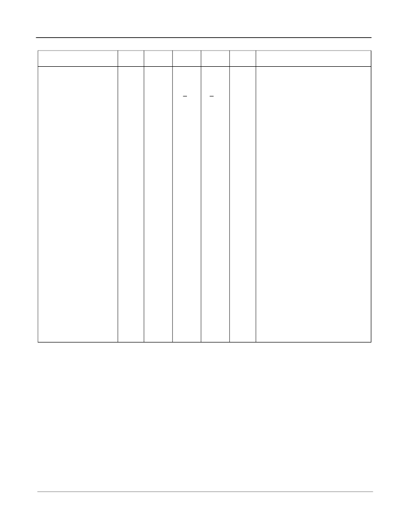
Characteristic
Pin
Min.
Typ.
Max.
Units
Conditions
Charge pump output
current
16
See Table 6.
Vpin16 = 2 V
Charge pump output
leakage
16
+3
+10
nA
Vpin16 = 2 V
Charge pump drive
output current
15
0.5
mA
Vpin15 = 0.7 V
Crystal frequency
17,
18
4
16
MHz
Application as in Figure 6.
Recommended crystal
series resonance
10
200
4 MHz parallel resonant crystal.
External reference input
frequency
17,
18
4
20
MHz
Sinewave coupled through 10 nF
blocking capacitor.
External reference drive
level
18
0.2
0.5
Vpp
Sinewave coupled through 10 nF
blocking capacitor.
Phase detector
comparison frequency
.03125
0.25
MHz
Equivalent phase noise
at phase detector
-158
With 4 MHz crystal, SSB, within loop
bandwidth.
With Fcomp = 125 kHz
RF division ratio
240
32767
Reference division ratio
See Table 1.
Switching ports P0-P3
sink current
leakage current
1, 5,
6, 14
10
10
mA
μ
A
Vport = 0.7 V
Vport = Vcc
Address select
Input high current
Input low current
24
1
-0.5
mA
mA
See Table 4.
Vin=Vcc
Vin=Vee
相關(guān)PDF資料 |
PDF描述 |
|---|---|
| SL2610LH1Q | Wide Dynamic Range Image Reject MOPLL |
| SL2610LH2N | Wide Dynamic Range Image Reject MOPLL |
| SL2610LH2Q | Wide Dynamic Range Image Reject MOPLL |
| SL3145 | 1.6GHz NPN TRANSISTOR ARRAYS |
| SL3145CMP | 1.6GHz NPN TRANSISTOR ARRAYS |
相關(guān)代理商/技術(shù)參數(shù) |
參數(shù)描述 |
|---|---|
| SL2610LH1Q | 制造商:ZARLINK 制造商全稱:Zarlink Semiconductor Inc 功能描述:Wide Dynamic Range Image Reject MOPLL |
| SL2610LH2N | 制造商:ZARLINK 制造商全稱:Zarlink Semiconductor Inc 功能描述:Wide Dynamic Range Image Reject MOPLL |
| SL2610LH2Q | 制造商:ZARLINK 制造商全稱:Zarlink Semiconductor Inc 功能描述:Wide Dynamic Range Image Reject MOPLL |
| SL2612313-6-BG | 制造商:Selecta Switch 功能描述: |
| SL262 | 制造商:Pass & Seymour/Legrand 功能描述:PLATE SS430 2G 2 SPLEX W/OUT LINE |
發(fā)布緊急采購(gòu),3分鐘左右您將得到回復(fù)。