- 您現(xiàn)在的位置:買賣IC網(wǎng) > PDF目錄374769 > SED1520D0A (Electronic Theatre Controls, Inc.) DOT MATRIX LCD DRIVER PDF資料下載
參數(shù)資料
| 型號: | SED1520D0A |
| 廠商: | Electronic Theatre Controls, Inc. |
| 英文描述: | DOT MATRIX LCD DRIVER |
| 中文描述: | 點陣液晶驅(qū)動 |
| 文件頁數(shù): | 20/52頁 |
| 文件大小: | 204K |
| 代理商: | SED1520D0A |
第1頁第2頁第3頁第4頁第5頁第6頁第7頁第8頁第9頁第10頁第11頁第12頁第13頁第14頁第15頁第16頁第17頁第18頁第19頁當前第20頁第21頁第22頁第23頁第24頁第25頁第26頁第27頁第28頁第29頁第30頁第31頁第32頁第33頁第34頁第35頁第36頁第37頁第38頁第39頁第40頁第41頁第42頁第43頁第44頁第45頁第46頁第47頁第48頁第49頁第50頁第51頁第52頁
3.2 – 3.2.2
3.0 Pin Configuration
S-MOS Systems, Inc. 150 River Oaks Parkway San Jose, CA 95134 Tel: (408) 922-0200 Fax: (408) 922-0238
371-1.0
20
3.2
PIN DESCRIPTION
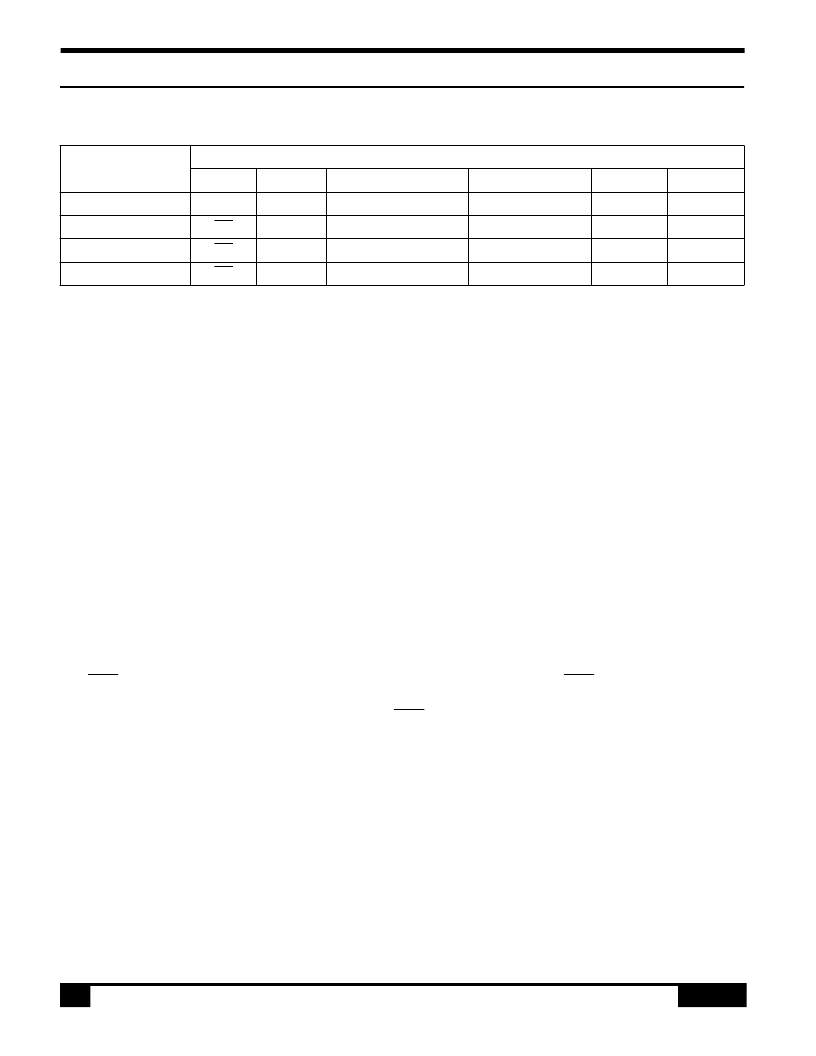
* Master LSI common outputs COM0–COM15 correspond to slave LSI outputs COM31–COM16.
3.2.1 Power Signals
V
DD
Connected to +5V power. Common to MPU power pin V
CC
.
V
SS
0V, connected to system GND.
V
1
–V
5
Multi-level power used to drive LCDs. Voltage specified to each LCD cell is divided by
resistors or impedance-converted by an operational amplifier before being applied. Each
voltage to be applied must be based on V
DD
, while fulfilling the following conditions:
V
DD
≥
V
1
≥
V
2
≥
V
3
≥
V
4
≥
V
5
3.2.2 System Bus Interface Signals
D
7
–D
0
8–bit, tri-state, bi-directional I/O bus. Normally, connected to the data bus of an 8–/16–
bit standard microcomputer.
A0
Input pin. Normally, the LSB of the MPU address bus is connected to this input pin to
provide data/command selection.
0: Display control data on D
7
–D
0
1: Display data on D
7
–D
0
RES
Input pin. The SED1520 can be reset or initialized by setting RES to low level (if it is
interfaced with a 68 family MPU) or high level (if with an 80 family MPU). This reset op-
eration occurs when an edge of the RES signal is sensed. The level input selects the
type of interface with the 68 or 80 family MPU:
High level: Interface with 68 family MPU
Low level:
Interface with 80 family MPU
Product name
Pin No.
74
75
96~100, 1~11
93
94
95
SED1520FOA
OSC1
OSC2
COM0~COM15*
M/S
V
4
V
1
SED1521FOA
CS
CL
SEG76~SEG61
SEG79
SEG78
SEG77
SED1520FAA
CS
CL
COM0~COM15*
M/S
V
4
V
1
SED1521FAA
CS
CL
SEG76~SEG61
SEG79
SEG78
SEG77
相關(guān)PDF資料 |
PDF描述 |
|---|---|
| SED1521 | DOT MATRIX LCD DRIVER |
| SED1600 | CMOS 80-SEGMENT LCD DRIVER |
| SED1600D | CMOS 80-SEGMENT LCD DRIVER |
| SED1600DAA | CMOS 80-SEGMENT LCD DRIVER |
| SED1600DAB | CMOS 80-SEGMENT LCD DRIVER |
相關(guān)代理商/技術(shù)參數(shù) |
參數(shù)描述 |
|---|---|
| SED1521 | 制造商:未知廠家 制造商全稱:未知廠家 功能描述:DOT MATRIX LCD DRIVER |
| SED1526 | 制造商:EPSON 制造商全稱:EPSON 功能描述:Dot Matrix LCD Controller Driver |
| SED1526F0A | 制造商:EPSON 制造商全稱:EPSON 功能描述:Dot Matrix LCD Controller Driver |
| SED1526FAA | 制造商:EPSON 制造商全稱:EPSON 功能描述:Dot Matrix LCD Controller Driver |
| SED1526FEA | 制造商:EPSON 制造商全稱:EPSON 功能描述:Dot Matrix LCD Controller Driver |
發(fā)布緊急采購,3分鐘左右您將得到回復(fù)。