- 您現(xiàn)在的位置:買(mǎi)賣(mài)IC網(wǎng) > PDF目錄372103 > SA56606-31GW (NXP SEMICONDUCTORS) CMOS system reset PDF資料下載
參數(shù)資料
| 型號(hào): | SA56606-31GW |
| 廠商: | NXP SEMICONDUCTORS |
| 元件分類(lèi): | 電源管理 |
| 英文描述: | CMOS system reset |
| 中文描述: | 1-CHANNEL POWER SUPPLY SUPPORT CKT, PDSO5 |
| 封裝: | PLASTIC, SOT-23, 5 PIN |
| 文件頁(yè)數(shù): | 7/12頁(yè) |
| 文件大?。?/td> | 122K |
| 代理商: | SA56606-31GW |
Philips Semiconductors
Product data
SA56606-XX
CMOS system reset
2001 Jun 19
7
TECHNICAL DESCRIPTION
The SA56606-XX is a CMOS device designed to provide power
source monitoring and a system reset function in the event the
supply voltage sags below an acceptable level for the system to
reliably operate. The device is designed to generate a compatible
reset signal for a wide variety of microprocessor and logic systems.
The SA56606 can operate at voltages up to 12 volts. The series
includes several versions providing precision threshold voltage reset
values of 2.0, 2.7, 2.8, 2.9, 3.0, 3.1, 4.2, 4.6 and 4.7 V. The reset
threshold incorporates a typical hysteresis of (V
S
×
0.05) volts to
prevent erratic resets from being generated.
The output of the SA56606 utilizes a low side open drain topology,
which requires an external pull-up resistor (R
PU
) to the V
DD
power
source. Although this may be regarded as a disadvantage, it is an
advantage in many sensitive applications because the open drain
output cannot source reset current to a microprocessor when both
are operated from a common supply. For this reason the SA56606
offers a safe inter-connect to a wide variety of microprocessors.
The SA56606 operates at very low supply currents, typically
0.25
μ
A, while offering a high precision of threshold detection (
±
2%).
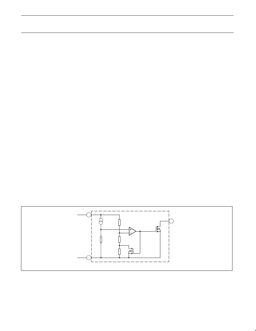
Figure 12 is a functional block diagram of the SA56606. The internal
reference source voltage (V
REF
) is typically 0.8 V over the operating
temperature range. The reference voltage is connected to the
non-inverting input of the threshold comparator, while the inverting
input monitors the supply voltage through a resistor divider network
made up of R
1
, R
2
, and R
3
. The output of the threshold comparator
drives the output Open Drain N-Channel FET of the device TR
1
).
When the supply voltage sags to the threshold detection voltage, the
resistor divider network supplies a voltage to the inverting input of
the threshold comparator, which is less than that of V
REF
, causing
the output of the comparator to go to a HIGH output state. This
causes the low side N-Channel FET to be active ON, pulling its
drain voltage to a LOW state. The device adheres to a true
input/output logic protocol: the output goes LOW when input is LOW
(below threshold) and output goes HIGH when input is HIGH (above
threshold).
The low side N-Channel FET (TR
2
) establishes threshold hysteresis
by turning ON whenever the threshold comparator’s output goes to
a HIGH state (when V
DD
sags to or below the threshold level). TR
2
’s
turning ON causes additional current to flow through resistors R
1
and
R
2
, causing the inverting input of the threshold comparator to be
pulled even lower. For the comparator to reverse its output polarity
and turn OFF TR
2
, the V
DD
source voltage must overcome this
additional pull-down voltage present on the comparator’s inverting
input. The differential voltage required to do this establishes the
hysteresis voltage of the sensed threshold voltage. Typically it is
(V
S
×
0.05) volts.
When the V
DD
voltage sags, and is at or below the Detection
Threshold (V
SL
), the device will assert a Reset LOW output at or
very near ground potential. As the V
DD
voltage rises from
(V
DD
< V
SL
) to V
SH
or higher, the Reset is released and the output
follows V
DD
. Conversely, decreases in V
DD
from (V
DD
> V
SL
) to V
SL
or lower cause the output to be pulled to ground.
Hysteresis Voltage = Release Voltage – Detection Threshold Voltage
V
HYS
= V
SH
– V
SL
where:
V
SH
= V
SL
+ V
HYS
V
REF
(R
1
+ R
2
) / R
2
V
SL
= V
REF
(R
1
+ R
2
+ R
3
) / (R
2
+ R
3
)
When V
DD
drops to levels below the minimum operating voltage,
typically less than 0.95 volts, the output is undefined and output
reset LOW assertion is not guaranteed. At this level of V
DD
the
output will try to rise to V
DD
.
The V
REF
voltage is typically 0.8 V. The devices are fabricated using
a high resistance CMOS process and utilize high resistance R
1
, R
2
,
and R
3
values requiring very small amounts of current. This
combination achieves very efficient low power performance over the
full operating temperature.
SL01323
V
DD
V
SS
V
REF
SA56606-XX
V
OUT
1
R
2
R
1
R
R
3
TR
1
TR
2
3
2
Figure 12. Functional diagram.
相關(guān)PDF資料 |
PDF描述 |
|---|---|
| SA56606-42 | CMOS system reset |
| SA56606-42GW | CMOS system reset |
| SA56606-43 | CMOS system reset |
| SA56606-43GW | CMOS system reset |
| SA56606-44 | CMOS system reset |
相關(guān)代理商/技術(shù)參數(shù) |
參數(shù)描述 |
|---|---|
| SA56606-42 | 制造商:PHILIPS 制造商全稱(chēng):NXP Semiconductors 功能描述:CMOS system reset |
| SA56606-42GW | 制造商:PHILIPS 制造商全稱(chēng):NXP Semiconductors 功能描述:CMOS system reset |
| SA56606-43 | 制造商:PHILIPS 制造商全稱(chēng):NXP Semiconductors 功能描述:CMOS system reset |
| SA56606-43GW | 制造商:PHILIPS 制造商全稱(chēng):NXP Semiconductors 功能描述:CMOS system reset |
| SA56606-44 | 制造商:PHILIPS 制造商全稱(chēng):NXP Semiconductors 功能描述:CMOS system reset |
發(fā)布緊急采購(gòu),3分鐘左右您將得到回復(fù)。