- 您現(xiàn)在的位置:買(mǎi)賣IC網(wǎng) > PDF目錄372103 > SA56606-30GW (NXP SEMICONDUCTORS) CMOS system reset PDF資料下載
參數(shù)資料
| 型號(hào): | SA56606-30GW |
| 廠商: | NXP SEMICONDUCTORS |
| 元件分類: | 電源管理 |
| 英文描述: | CMOS system reset |
| 中文描述: | 1-CHANNEL POWER SUPPLY SUPPORT CKT, PDSO5 |
| 封裝: | PLASTIC, SOT-23, 5 PIN |
| 文件頁(yè)數(shù): | 8/12頁(yè) |
| 文件大?。?/td> | 122K |
| 代理商: | SA56606-30GW |
Philips Semiconductors
Product data
SA56606-XX
CMOS system reset
2001 Jun 19
8
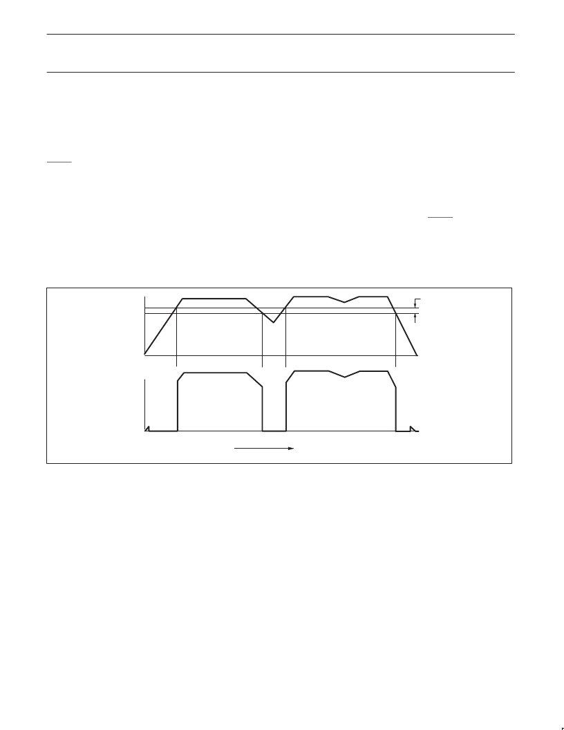
Timing diagram
The timing diagram shown in Figure 13 depicts the operation of the
device. Letters A–J on the TIME axis indicate specific events.
A:
increases but abruptly decreases when V
DD
reaches the level
(approximately 0.8 V) that activates the internal bias circuitry and
RESET is asserted.
At ‘A’, V
DD
begins to increase. Also the V
OUT
voltage initially
B:
device releases the hold on the V
OUT
reset. The Reset output V
OUT
tracks V
DD
as it rises above V
SH
(assuming the reset pull-up resistor
R
PU
is connected to V
DD
). In a microprocessor based system these
events release the reset from the microprocessor, allowing the
microprocessor to function normally.
At ‘B’, V
DD
reaches the threshold level of V
SH
. At this point the
C–D:
continues to fall until the V
SL
undervoltage detection threshold is
reached at ‘D’. This causes a reset signal to be generated (V
OUT
Reset goes LOW).
At ‘C’, V
DD
begins to fall, causing V
OUT
to follow. V
DD
D–E:
Between ‘D’ and ‘E’, V
DD
starts rising.
E:
the hold on the V
OUT
reset. The Reset output V
OUT
tracks V
DD
as it
rises above V
SH
.
At ‘E’, V
DD
rises to the V
SH
. Once again, the device releases
F–G:
causing V
OUT
to follow it. As long as V
DD
remains above the V
SH
,
no reset signal will be triggered. Before V
DD
falls to the V
SH
, it
begins to rise, causing V
OUT
to follow it. At ‘G’, V
DD
returns to
normal.
At ‘F’, V
DD
is above the upper threshold and begins to fall,
H:
threshold point is reached. At this level, a RESET signal is
generated and V
OUT
goes LOW.
At event ‘H’ V
DD
falls until the V
SL
undervoltage detection
J:
bias is unable to maintain a V
OUT
reset. As a result, V
DD
may rise to
less than 0.8 V. As V
DD
decreases further, V
OUT
reset also
decreases to zero.
At ‘J’ the V
DD
voltage has decreased until normal internal circuit
SL01354
V
DD
V
OUT
TIME
V
SH
V
SL
0
0
A
B
C
G
H
J
D
E
F
V
S
Figure 13. Timing diagram.
相關(guān)PDF資料 |
PDF描述 |
|---|---|
| SA56606-31 | CMOS system reset |
| SA56606-31GW | CMOS system reset |
| SA56606-42 | CMOS system reset |
| SA56606-42GW | CMOS system reset |
| SA56606-43 | CMOS system reset |
相關(guān)代理商/技術(shù)參數(shù) |
參數(shù)描述 |
|---|---|
| SA56606-31 | 制造商:PHILIPS 制造商全稱:NXP Semiconductors 功能描述:CMOS system reset |
| SA56606-31GW | 制造商:PHILIPS 制造商全稱:NXP Semiconductors 功能描述:CMOS system reset |
| SA56606-42 | 制造商:PHILIPS 制造商全稱:NXP Semiconductors 功能描述:CMOS system reset |
| SA56606-42GW | 制造商:PHILIPS 制造商全稱:NXP Semiconductors 功能描述:CMOS system reset |
| SA56606-43 | 制造商:PHILIPS 制造商全稱:NXP Semiconductors 功能描述:CMOS system reset |
發(fā)布緊急采購(gòu),3分鐘左右您將得到回復(fù)。