- 您現(xiàn)在的位置:買賣IC網(wǎng) > PDF目錄286180 > BYAP80-50 TOGGLE SWITCH, DP3T, MOMENTARY, 4A, 28VDC, PANEL MOUNT-THREADED PDF資料下載
參數(shù)資料
| 型號: | BYAP80-50 |
| 元件分類: | 開關 |
| 英文描述: | TOGGLE SWITCH, DP3T, MOMENTARY, 4A, 28VDC, PANEL MOUNT-THREADED |
| 文件頁數(shù): | 1/7頁 |
| 文件大小: | 525K |
| 代理商: | BYAP80-50 |
A-78
APEM
www.apem.com
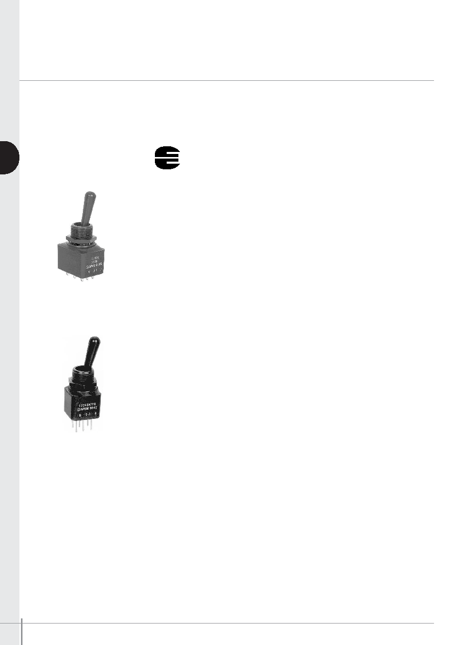
12000X778 series
High performance toggle switches - threaded bushing 11,9 (15/32)
Distinctive features
A
K
Approval and lists
CECC 96201-005
CECC 96201-008
MUAHAG and QPL listed (Europe only)
French defence approved : DAT list No A5999 X001.
This range of professional toggle switches is suitable for use in military and
other high specification environments.
K
Contacts
Highly reliable contacts suitable for low level applications (10mA 50mV -
10A 5VDC min.) or power applications (2A 250VAC - 4A 125VAC -
4A 30VDC max.)
K
Pinned lever
The base of the switch lever is pinned to the bushing, thus earthing the lever to
the bushing. This also provides strain relief to protect the switch if accidentally
knocked.
K
Double shell case
For high mechanical strength and high electrical insulation.
K
Compact size
The small rear end of the switch allows space saving behind the panel.
K
Finish
Matt black finish on body, bushing, lever and hardware.
K
Sealing
Panel sealed to IP 67, these switches are frontal sealed by two O-rings and
have full rear end sealing.
K
Accessories
A comprehensive range of protection boots (both full and half length), locking
levers and security caps are available.
相關PDF資料 |
PDF描述 |
|---|---|
| BYAP80-500 | TOGGLE SWITCH, DP3T, MOMENTARY, 4A, 28VDC, PANEL MOUNT-THREADED |
| BYAP80-500R | TOGGLE SWITCH, DP3T, MOMENTARY, 4A, 28VDC, PANEL MOUNT-THREADED |
| BYAP80-50R | TOGGLE SWITCH, DP3T, MOMENTARY, 4A, 28VDC, PANEL MOUNT-THREADED |
| BYP150-100 | TOGGLE SWITCH, DP3T, MOMENTARY, 4A, 28VDC, PANEL MOUNT-THREADED |
| BYP150-225 | TOGGLE SWITCH, DP3T, MOMENTARY, 4A, 28VDC, PANEL MOUNT-THREADED |
相關代理商/技術參數(shù) |
參數(shù)描述 |
|---|---|
| BYAP80-500 | 制造商:未知廠家 制造商全稱:未知廠家 功能描述:DIODY TYRYSTORY |
| BYAP80-500R | 制造商:未知廠家 制造商全稱:未知廠家 功能描述:DIODY TYRYSTORY |
| BYAP80-50R | 制造商:未知廠家 制造商全稱:未知廠家 功能描述:DIODY TYRYSTORY |
| BYC10600 | 制造商:FAIRCHILD 制造商全稱:Fairchild Semiconductor 功能描述:PFC+PWM Combination Controller |
| BYC10-600 | 功能描述:整流器 RAIL PN DIODE RoHS:否 制造商:Vishay Semiconductors 產(chǎn)品:Standard Recovery Rectifiers 配置: 反向電壓:100 V 正向電壓下降: 恢復時間:1.2 us 正向連續(xù)電流:2 A 最大浪涌電流:35 A 反向電流 IR:5 uA 安裝風格:SMD/SMT 封裝 / 箱體:DO-221AC 封裝:Reel |
發(fā)布緊急采購,3分鐘左右您將得到回復。