- 您現(xiàn)在的位置:買賣IC網(wǎng) > PDF目錄225141 > S29JL032H90TAI223 (ADVANCED MICRO DEVICES INC) 2M X 16 FLASH 3V PROM, 90 ns, PDSO48 PDF資料下載
參數(shù)資料
| 型號(hào): | S29JL032H90TAI223 |
| 廠商: | ADVANCED MICRO DEVICES INC |
| 元件分類: | PROM |
| 英文描述: | 2M X 16 FLASH 3V PROM, 90 ns, PDSO48 |
| 封裝: | MO-142DD, TSOP-48 |
| 文件頁數(shù): | 35/66頁 |
| 文件大?。?/td> | 1691K |
| 代理商: | S29JL032H90TAI223 |
第1頁第2頁第3頁第4頁第5頁第6頁第7頁第8頁第9頁第10頁第11頁第12頁第13頁第14頁第15頁第16頁第17頁第18頁第19頁第20頁第21頁第22頁第23頁第24頁第25頁第26頁第27頁第28頁第29頁第30頁第31頁第32頁第33頁第34頁當(dāng)前第35頁第36頁第37頁第38頁第39頁第40頁第41頁第42頁第43頁第44頁第45頁第46頁第47頁第48頁第49頁第50頁第51頁第52頁第53頁第54頁第55頁第56頁第57頁第58頁第59頁第60頁第61頁第62頁第63頁第64頁第65頁第66頁
38
S29JL032H
S29JL032H_00A11 March 10, 2005
Advan ce
In form ati o n
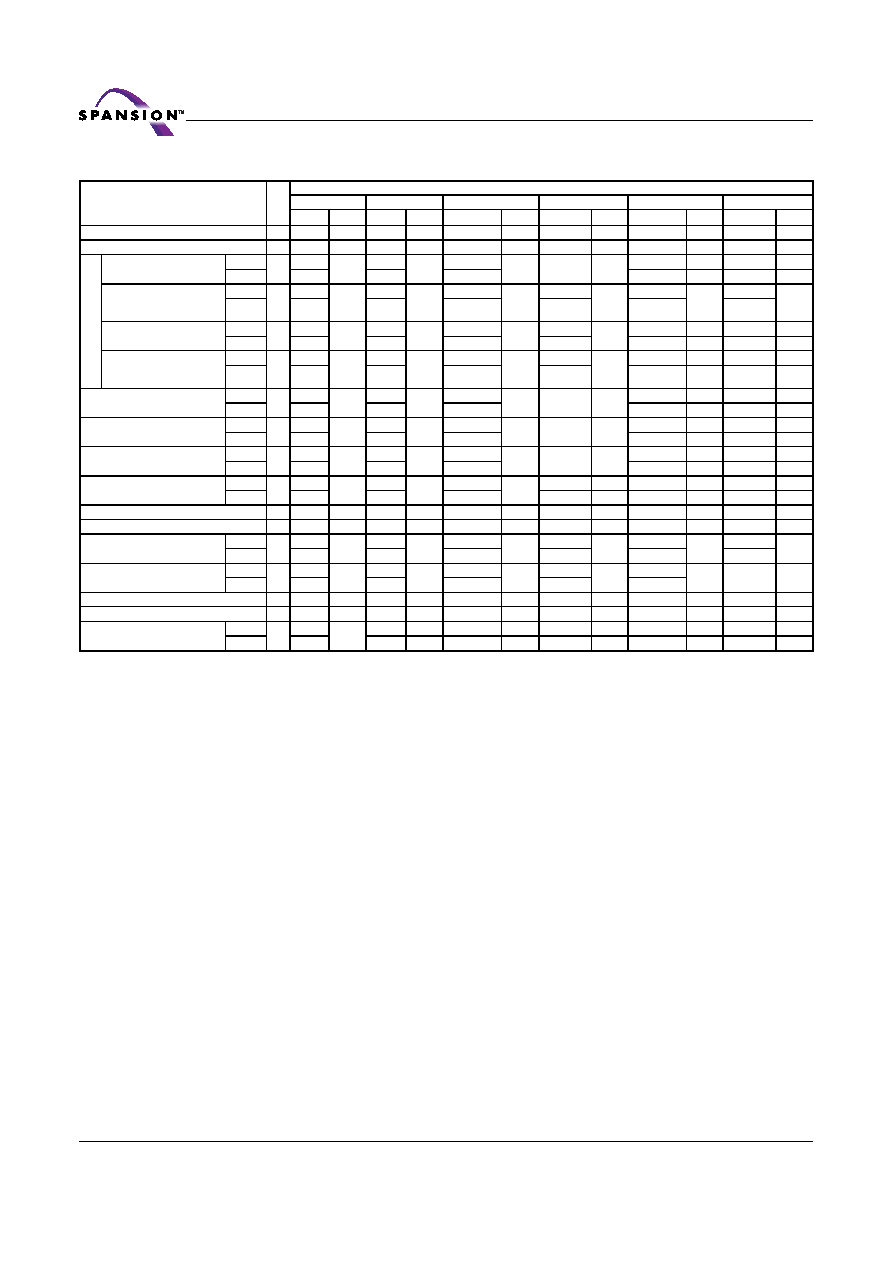
Table 13. S29JL032H Command Definitions
Command
Sequence
Cyc
le
s
Bus Cycles (Notes 2–5)
First
Second
Third
Fourth
Fifth
Sixth
Addr Data Addr Data
Addr
Data
Addr
Data
Addr
Data
Addr
Data
Read (Note 6)
1
RA
RD
Reset (Note 7)
1
XXX
F0
Au
to
se
le
ct
Manufacturer ID
Word
4
555
AA
2AA
55
(BA)555
90
(BA)X00
01
Byte
AAA
555
(BA)AAA
Device ID (Note 9)
Word
6
555
AA
2AA
55
(BA)555
90
(BA)X01
See
(BA)X0E
See
(BA)X0F
See
Byte
AAA
555
(BA)AAA
(BA)X02
(BA)X1C
(BA)X1E
SecSi Sector Factory
Protect (Note 10)
Word
4
555
AA
2AA
55
(BA)555
90
(BA)X03
82/
02
Byte
AAA
555
(BA)AAA
(BA)X06
Sector/Sector Block
Protect Verify
Word
4
555
AA
2AA
55
(BA)555
90
(SA)X02
00/
01
Byte
AAA
555
(BA)AAA
(SA)X04
Enter SecSi Sector Region
Word
3
555
AA
2AA
55
555
88
Byte
AAA
555
AAA
Exit SecSi Sector Region
Word
4
555
AA
2AA
55
555
90
XXX
00
Byte
AAA
555
AAA
Program
Word
4
555
AA
2AA
55
555
A0
PA
PD
Byte
AAA
555
AAA
Unlock Bypass
Word
3
555
AA
2AA
55
555
20
Byte
AAA
555
AAA
Unlock Bypass Program (Note 12)
2
XXX
A0
PA
PD
Unlock Bypass Reset (Note 13)
2
XXX
90
XXX
00
Chip Erase
Word
6
555
AA
2AA
55
555
80
555
AA
2AA
55
555
10
Byte
AAA
555
AAA
555
AAA
Sector Erase
Word
6
555
AA
2AA
55
555
80
555
AA
2AA
55
SA
30
Byte
AAA
555
AAA
555
Erase Suspend (Note 14)
1
BA
B0
Erase Resume (Note 15)
1
BA
30
CFI Query (Note 16)
Word
1
55
98
Byte
AA
Legend:
X = Don’t care
RA = Address of the memory location to be read.
RD = Data read from location RA during read operation.
PA = Address of the memory location to be programmed. Addresses
latch on the falling edge of the WE# or CE# pulse, whichever happens
later.
PD = Data to be programmed at location PA. Data latches on the rising
edge of WE# or CE# pulse, whichever happens first.
SA = Address of the sector to be verified (in autoselect mode) or
erased. Address bits A20–A12 uniquely select any sector. Refer to
BA = Address of the bank that is being switched to autoselect mode, is
in bypass mode, or is being erased. A20–A18 uniquely select a bank.
Notes:
1. See Table 1 for description of bus operations.
2. All values are in hexadecimal.
3. Except for the read cycle and the fourth, fifth, and sixth cycle of
the autoselect command sequence, all bus cycles are write
cycles.
4. Data bits DQ15–DQ8 are don’t care in command sequences,
except for RD and PD.
5. Unless otherwise noted, address bits A20–A11 are don’t cares for
unlock and command cycles, unless SA or PA is required.
6. No unlock or command cycles required when bank is reading
array data.
7. The Reset command is required to return to the read mode (or to
the erase-suspend-read mode if previously in Erase Suspend)
when a bank is in the autoselect mode, or if DQ5 goes high
(while the bank is providing status information).
8. The fourth cycle of the autoselect command sequence is a read
cycle. The system must provide the bank address to obtain the
manufacturer ID, device ID, or SecSi Sector factory protect
information. Data bits DQ15–DQ8 are don’t care. While reading
the autoselect addresses, the bank address must be the same
until a reset command is given. See the Autoselect Command
Sequence section for more information.
9. For models 01, 02, the device ID must be read across the fourth,
fifth, and sixth cycles.
10. The data is 82h for factory locked, 42h for customer locked, and
02h for not factory/customer locked.
11. The data is 00h for an unprotected sector/sector block and 01h
for a protected sector/sector block.
12. The Unlock Bypass command is required prior to the Unlock
Bypass Program command.
13. The Unlock Bypass Reset command is required to return to the
read mode when the bank is in the unlock bypass mode.
14. The system may read and program in non-erasing sectors, or
enter the autoselect mode, when in the Erase Suspend mode.
The Erase Suspend command is valid only during a sector erase
operation, and requires the bank address.
15. The Erase Resume command is valid only during the Erase
Suspend mode, and requires the bank address.
16. Command is valid when device is ready to read array data or
when device is in autoselect mode.
相關(guān)PDF資料 |
PDF描述 |
|---|---|
| S29WS064N0PBAW011 | 256/128/64 MEGABIT CMOS 1.8 VOLT ONLY SIMULTANEOUS READ/WRITE BURST MODE FLASH MEMORY |
| S29WS128N0LBFI111 | 256/128/64 MEGABIT CMOS 1.8 VOLT ONLY SIMULTANEOUS READ/WRITE BURST MODE FLASH MEMORY |
| S29WS128N0LBFI112 | 256/128/64 MEGABIT CMOS 1.8 VOLT ONLY SIMULTANEOUS READ/WRITE BURST MODE FLASH MEMORY |
| S29WS128N0LBFI113 | 256/128/64 MEGABIT CMOS 1.8 VOLT ONLY SIMULTANEOUS READ/WRITE BURST MODE FLASH MEMORY |
| S29WS128N0LBFW011 | Test Clip; Current Rating:100A; Body Material:Steel; Features:Unmarked; Jaw Opening Max:1.625"; Overall Length:6" RoHS Compliant: NA |
相關(guān)代理商/技術(shù)參數(shù) |
參數(shù)描述 |
|---|---|
| S29JL032H90TAI310 | 功能描述:閃存 3V 32Mb Float Gate top boot 2Banks 90s RoHS:否 制造商:ON Semiconductor 數(shù)據(jù)總線寬度:1 bit 存儲(chǔ)類型:Flash 存儲(chǔ)容量:2 MB 結(jié)構(gòu):256 K x 8 定時(shí)類型: 接口類型:SPI 訪問時(shí)間: 電源電壓-最大:3.6 V 電源電壓-最小:2.3 V 最大工作電流:15 mA 工作溫度:- 40 C to + 85 C 安裝風(fēng)格:SMD/SMT 封裝 / 箱體: 封裝:Reel |
| S29JL032H90TAI311 | 制造商:SPANSION 制造商全稱:SPANSION 功能描述:32M BIT CMOS 3.0V FLASH MEMORY |
| S29JL032H90TAI312 | 制造商:SPANSION 制造商全稱:SPANSION 功能描述:32M BIT CMOS 3.0V FLASH MEMORY |
| S29JL032H90TAI313 | 功能描述:閃存 3V 32M SIMULTANEOUS READ/WRITE FLASH RoHS:否 制造商:ON Semiconductor 數(shù)據(jù)總線寬度:1 bit 存儲(chǔ)類型:Flash 存儲(chǔ)容量:2 MB 結(jié)構(gòu):256 K x 8 定時(shí)類型: 接口類型:SPI 訪問時(shí)間: 電源電壓-最大:3.6 V 電源電壓-最小:2.3 V 最大工作電流:15 mA 工作溫度:- 40 C to + 85 C 安裝風(fēng)格:SMD/SMT 封裝 / 箱體: 封裝:Reel |
| S29JL032H90TAI320 | 功能描述:閃存 3V 32Mb Float Gate btm boot 2Banks 90s RoHS:否 制造商:ON Semiconductor 數(shù)據(jù)總線寬度:1 bit 存儲(chǔ)類型:Flash 存儲(chǔ)容量:2 MB 結(jié)構(gòu):256 K x 8 定時(shí)類型: 接口類型:SPI 訪問時(shí)間: 電源電壓-最大:3.6 V 電源電壓-最小:2.3 V 最大工作電流:15 mA 工作溫度:- 40 C to + 85 C 安裝風(fēng)格:SMD/SMT 封裝 / 箱體: 封裝:Reel |
發(fā)布緊急采購,3分鐘左右您將得到回復(fù)。