- 您現(xiàn)在的位置:買賣IC網(wǎng) > PDF目錄203263 > VTC4-D45D-14M7456 (VECTRON INTERNATIONAL) TCVCXO, CLIPPED SINE OUTPUT, 14.7456 MHz PDF資料下載
參數(shù)資料
| 型號: | VTC4-D45D-14M7456 |
| 廠商: | VECTRON INTERNATIONAL |
| 元件分類: | TCVCXO, sine |
| 英文描述: | TCVCXO, CLIPPED SINE OUTPUT, 14.7456 MHz |
| 文件頁數(shù): | 1/7頁 |
| 文件大小: | 173K |
| 代理商: | VTC4-D45D-14M7456 |
Vectron International 267 Lowell Road, Hudson NH 03051
Tel: 1-88-VECTRON-1
e-mail: vectron@vectron.com
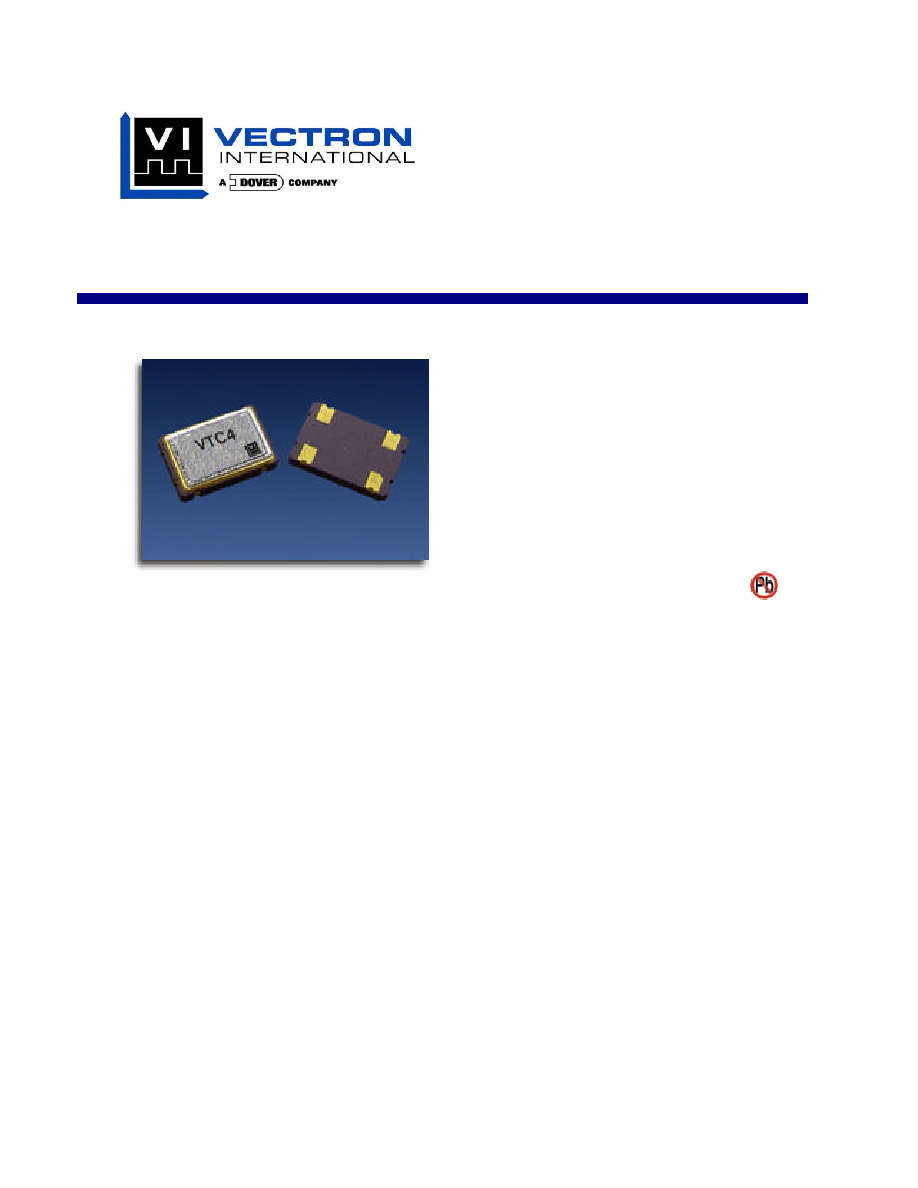
VTC4 series
Voltage Controlled Temperature Compensated Crystal Oscillator
The VTC4, VCTXCO
Features
Clipped Sine Wave Output
Output Frequencies to 27 MHz
Fundamental Crystal Design
Optional VCXO Function available
Gold over nickel contact pads
Hermetically Sealed Ceramic SMD package
Product is compliant to RoHS directive
and fully compatible with lead free assembly
Applications
Wireless Communications
Base Stations
Point to point radios
Broadband Access
Test Equipment
Handsets
Description
Vectron’s VTC4 Temperature Compensated
Crystal Oscillator (TCXO) is a quartz stabilized,
clipped sine wave output, temperature
compensated oscillator, operating off either 2.8,
3.0, 3.3 or 5.0 volt supply.
相關PDF資料 |
PDF描述 |
|---|---|
| VTC4-D45E-24M5535 | TCVCXO, CLIPPED SINE OUTPUT, 24.5535 MHz |
| VTC4-D53A-24M5535 | TCVCXO, CLIPPED SINE OUTPUT, 24.5535 MHz |
| VTC4-C5BA-15M000 | TCVCXO, CLIPPED SINE OUTPUT, 15 MHz |
| VTC4-C5BB-24M576 | TCVCXO, CLIPPED SINE OUTPUT, 24.576 MHz |
| VTC4-C5BE-12M504 | TCVCXO, CLIPPED SINE OUTPUT, 12.504 MHz |
相關代理商/技術參數(shù) |
參數(shù)描述 |
|---|---|
| VTC5260H1 | 制造商:CPI 制造商全稱:CPI 功能描述:TWT |
| VTC5262B1K | 制造商:CPI 制造商全稱:CPI 功能描述:Long life C-Band TWT suitable for use in weather radars. |
| VTC5760B | 制造商:CPI 制造商全稱:CPI 功能描述:VTC-5760B Pulsed Coupled Cavity TWT |
| VTC5762A | 制造商:CPI 制造商全稱:CPI 功能描述:VTC-5762A Pulsed Coupled Cavity TWT |
| VTC-5762B5 | 制造商:CPI 制造商全稱:CPI 功能描述:5.2 to 5.9 GHz |
發(fā)布緊急采購,3分鐘左右您將得到回復。