- 您現(xiàn)在的位置:買賣IC網(wǎng) > PDF目錄371105 > MH16S72BAMD-6 (Mitsubishi Electric Corporation) 1,207,959,552-BIT ( 16,777,216-WORD BY 72-BIT ) Synchronous DYNAMIC RAM PDF資料下載
參數(shù)資料
| 型號(hào): | MH16S72BAMD-6 |
| 廠商: | Mitsubishi Electric Corporation |
| 英文描述: | 1,207,959,552-BIT ( 16,777,216-WORD BY 72-BIT ) Synchronous DYNAMIC RAM |
| 中文描述: | 1207959552位(16,777,216字72位)同步動(dòng)態(tài)隨機(jī)存儲(chǔ)器 |
| 文件頁(yè)數(shù): | 22/52頁(yè) |
| 文件大?。?/td> | 1045K |
| 代理商: | MH16S72BAMD-6 |
第1頁(yè)第2頁(yè)第3頁(yè)第4頁(yè)第5頁(yè)第6頁(yè)第7頁(yè)第8頁(yè)第9頁(yè)第10頁(yè)第11頁(yè)第12頁(yè)第13頁(yè)第14頁(yè)第15頁(yè)第16頁(yè)第17頁(yè)第18頁(yè)第19頁(yè)第20頁(yè)第21頁(yè)當(dāng)前第22頁(yè)第23頁(yè)第24頁(yè)第25頁(yè)第26頁(yè)第27頁(yè)第28頁(yè)第29頁(yè)第30頁(yè)第31頁(yè)第32頁(yè)第33頁(yè)第34頁(yè)第35頁(yè)第36頁(yè)第37頁(yè)第38頁(yè)第39頁(yè)第40頁(yè)第41頁(yè)第42頁(yè)第43頁(yè)第44頁(yè)第45頁(yè)第46頁(yè)第47頁(yè)第48頁(yè)第49頁(yè)第50頁(yè)第51頁(yè)第52頁(yè)
MH16S72AMA -8,-10,-12
1207959552-BIT (16777216 - WORD BY 72-BIT)SynchronousDRAM
MITSUBISHI LSIs
( / 52 )
22
MITSUBISHI
ELECTRIC
5. Mar.1997
Preliminary Spec.
Some contents are subject to change without notice.
MIT-DS-0128-0.0
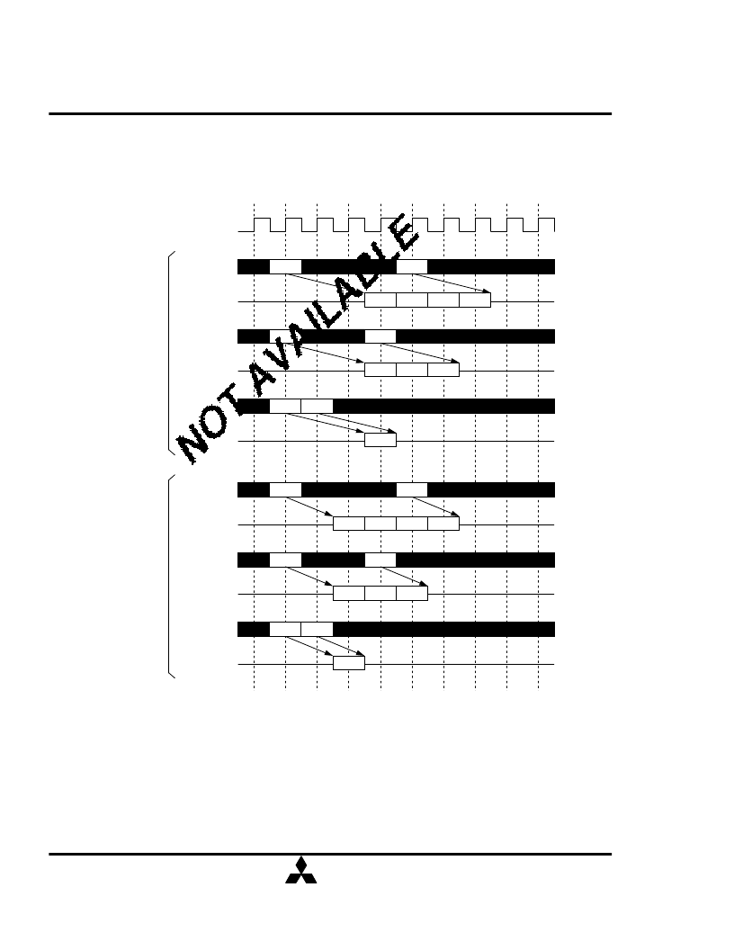
[ Read Interrupted by Burst Terminate ]
Similarly to the precharge, burst terminate command can interrupt burst read operation and
disable the data output. READ to TERM interval is minimum 1 CK. The figure below shows
examples, when the dataout is terminated.
Read Interrupted by Burst Terminate (BL=4)
CK
Command
DQ
READ
TERM
Q0
Q1
Q2
Q3
CL=3
Command
DQ
READ
TERM
Q0
Q1
Q2
Command
DQ
READ TERM
Q0
Command
DQ
READ
TERM
Q0
Q1
Q2
Q3
CL=2
Command
DQ
READ
TERM
Q0
Q1
Q2
Command
DQ
READ TERM
Q0
Comman
d
DQ
REA
D
TERM
Q
0
Q
1
Q
2
Q
3
CL=
1
Comman
d
DQ
REA
D
TERM
Q
0
相關(guān)PDF資料 |
PDF描述 |
|---|---|
| MH16S72BAMD-7 | 1207959552-BIT (16777216 - WORD BY 72-BIT)SynchronousDRAM |
| MH16S72BAMD-8 | 1207959552-BIT (16777216 - WORD BY 72-BIT)SynchronousDRAM |
| MH16S72BCFA-6 | 1,207,959,552-BIT ( 16,777,216-WORD BY 72-BIT ) Synchronous DYNAMIC RAM |
| MH16S72DAMD-6 | 1207959552-BIT (16777216 - WORD BY 72-BIT)Synchronous DRAM |
| MH16S72DAMD-7 | 1207959552-BIT (16777216 - WORD BY 72-BIT)Synchronous DRAM |
相關(guān)代理商/技術(shù)參數(shù) |
參數(shù)描述 |
|---|---|
| MH16S72BAMD-7 | 制造商:MITSUBISHI 制造商全稱:Mitsubishi Electric Semiconductor 功能描述:1207959552-BIT (16777216 - WORD BY 72-BIT)SynchronousDRAM |
| MH16S72BAMD-8 | 制造商:MITSUBISHI 制造商全稱:Mitsubishi Electric Semiconductor 功能描述:1207959552-BIT (16777216 - WORD BY 72-BIT)SynchronousDRAM |
| MH16S72BCFA-6 | 制造商:MITSUBISHI 制造商全稱:Mitsubishi Electric Semiconductor 功能描述:1,207,959,552-BIT ( 16,777,216-WORD BY 72-BIT ) Synchronous DYNAMIC RAM |
| MH16S72BDFA-7 | 制造商:MITSUBISHI 制造商全稱:Mitsubishi Electric Semiconductor 功能描述:1,207,959,552-BIT ( 16,777,216-WORD BY 72-BIT ) Synchronous DYNAMIC RAM |
| MH16S72BDFA-8 | 制造商:MITSUBISHI 制造商全稱:Mitsubishi Electric Semiconductor 功能描述:1,207,959,552-BIT ( 16,777,216-WORD BY 72-BIT ) Synchronous DYNAMIC RAM |
發(fā)布緊急采購(gòu),3分鐘左右您將得到回復(fù)。