- 您現(xiàn)在的位置:買賣IC網(wǎng) > PDF目錄296642 > MT58L512Y36FT-8.5 (CYPRESS SEMICONDUCTOR CORP) 512K X 36 CACHE SRAM, 8.5 ns, PQFP100 PDF資料下載
參數(shù)資料
| 型號(hào): | MT58L512Y36FT-8.5 |
| 廠商: | CYPRESS SEMICONDUCTOR CORP |
| 元件分類: | SRAM |
| 英文描述: | 512K X 36 CACHE SRAM, 8.5 ns, PQFP100 |
| 封裝: | PLASTIC, TQFP-100 |
| 文件頁(yè)數(shù): | 3/34頁(yè) |
| 文件大小: | 537K |
| 代理商: | MT58L512Y36FT-8.5 |
第1頁(yè)第2頁(yè)當(dāng)前第3頁(yè)第4頁(yè)第5頁(yè)第6頁(yè)第7頁(yè)第8頁(yè)第9頁(yè)第10頁(yè)第11頁(yè)第12頁(yè)第13頁(yè)第14頁(yè)第15頁(yè)第16頁(yè)第17頁(yè)第18頁(yè)第19頁(yè)第20頁(yè)第21頁(yè)第22頁(yè)第23頁(yè)第24頁(yè)第25頁(yè)第26頁(yè)第27頁(yè)第28頁(yè)第29頁(yè)第30頁(yè)第31頁(yè)第32頁(yè)第33頁(yè)第34頁(yè)
18Mb: 1 MEG x 18, 512K x 32/36
FLOW-THROUGH SYNCBURST SRAM
18Mb: 1 Meg x 18, 512K x 32/36, Flow-Through SyncBurst SRAM
Micron Technology, Inc., reserves the right to change products or specifications without notice.
MT58L1MY18F_16_D.fm – Rev. D, Pub. 2/03
11
2003 Micron Technology, Inc.
NOTE:
1. X means “Don’t Care.” # means active LOW. H means logic HIGH. L means logic LOW.
2. For WRITE#, L means any one or more byte write enable signals (BWa#, BWb#, BWc#, or BWd#) and BWE# are LOW
or GW# is LOW. WRITE# = H for all BWx#, BWE#, GW# HIGH.
3. BWa# enables writes to DQa pins/balls and DQPa. BWb# enables writes to DQb pins/balls and DQPb. BWc# enables
writes to DQc pins/balls and DQPc. BWd# enables writes to DQd pins/balls and DQPd. DQPa and DQPb are only avail-
able on the x18 and x36 versions. DQPc and DQPd are only available on the x36 version.
4. All inputs except OE# and ZZ must meet setup and hold times around the rising edge (LOW to HIGH) of CLK.
5. Wait states are inserted by suspending burst.
6. For a WRITE operation following a READ operation, OE# must be HIGH before the input data setup time and held
HIGH throughout the input data hold time.
7. This device contains circuitry that will ensure the outputs will be in High-Z during power-up.
8. ADSP# LOW always initiates an internal READ at the L–H edge of CLK. A WRITE is performed by setting one or more
byte write enable signals and BWE# LOW or GW# LOW for the subsequent L–H edge of CLK. Refer to WRITE timing
diagram for clarification.
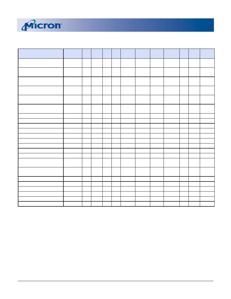
Table 7:
Truth Table
OPERATION
ADDRESS
USED
CE# CE2# CE2
ZZ
ADSP# ADSC#
ADV#
WRITE# OE#
CLK
DQ
Deselect Cycle, Power-
Down
None
H
X
L
X
L
X
L–H
High-Z
Deselect Cycle, Power-
Down
None
L
X
L
X
L–H
High-Z
Deselect Cycle, Power-
Down
None
L
H
X
L
X
L–H
High-Z
Deselect Cycle, Power-
Down
None
L
X
L
H
L
X
L–H
High-Z
Deselect Cycle, Power-
Down
None
L
H
X
L
H
L
X
L–H
High-Z
SNOOZE Mode, Power-
Down
None
X
H
X
High-Z
Read Cycle, Begin Burst
External
L
H
L
X
L
L–H
Q
Read Cycle, Begin Burst
External
L
H
L
X
H
L–H
High-Z
Write Cycle, Begin Burst
External
L
H
L
H
L
X
L
X
L–H
D
Read Cycle, Begin Burst
External
L
H
L
H
L
X
H
L
L–H
Q
Read Cycle, Begin Burst
External
L
H
L
H
L
X
H
L–H
High-Z
Read Cycle, Continue Burst
Next
X
L
H
L
H
L
L–H
Q
Read Cycle, Continue Burst
Next
X
L
H
L
H
L–H
High-Z
Read Cycle, Continue Burst
Next
H
X
L
X
H
L
H
L
L–H
Q
Read Cycle, Continue Burst
Next
H
X
L
X
H
L
H
L–H
High-Z
Write Cycle, Continue
Burst
Next
X
L
H
L
X
L–H
D
Write Cycle, Continue
Burst
Next
H
X
L
X
H
L
X
L–H
D
Read Cycle, Suspend Burst
Current
X
L
H
L
L–H
Q
Read Cycle, Suspend Burst
Current
X
L
H
L–H
High-Z
Read Cycle, Suspend Burst
Current
H
X
L
X
H
L
L–H
Q
Read Cycle, Suspend Burst
Current
H
X
L
X
H
L–H
High-Z
Write Cycle, Suspend Burst
Current
X
L
H
L
X
L–H
D
Write Cycle, Suspend Burst
Current
H
X
L
X
H
L
X
L–H
D
相關(guān)PDF資料 |
PDF描述 |
|---|---|
| MT58V1MV18DT-10 | 1M X 18 CACHE SRAM, 5 ns, PQFP100 |
| MT5C2565EC-70/IT | 64K X 4 STANDARD SRAM, 70 ns, CQCC28 |
| MT5C256K16B2DJ-12PAT | 256K X 16 STANDARD SRAM, 12 ns, PDSO54 |
| MT5C256K16B2DJ-35LAT | 256K X 16 STANDARD SRAM, 35 ns, PDSO54 |
| MT5C256K16B2TG-12L | 256K X 16 STANDARD SRAM, 12 ns, PDSO54 |
相關(guān)代理商/技術(shù)參數(shù) |
參數(shù)描述 |
|---|---|
| MT58L512Y36PF-10 | 制造商:Rochester Electronics LLC 功能描述:- Bulk |
| MT58L512Y36PF-6 | 制造商:Rochester Electronics LLC 功能描述:- Bulk |
| MT58L512Y36PT10 | 制造商:MT 功能描述:New |
| MT58L512Y36PT-5 | 制造商:Rochester Electronics LLC 功能描述:- Bulk 制造商:Micron Technology Inc 功能描述: |
| MT58L512Y36PT-6 | 制造商:Rochester Electronics LLC 功能描述:- Bulk 制造商:Micron Technology Inc 功能描述: |
發(fā)布緊急采購(gòu),3分鐘左右您將得到回復(fù)。