- 您現(xiàn)在的位置:買賣IC網(wǎng) > PDF目錄296642 > MT58L128L36P1T-5 (CYPRESS SEMICONDUCTOR CORP) 128K X 36 CACHE SRAM, 2.8 ns, PQFP100 PDF資料下載
參數(shù)資料
| 型號: | MT58L128L36P1T-5 |
| 廠商: | CYPRESS SEMICONDUCTOR CORP |
| 元件分類: | SRAM |
| 英文描述: | 128K X 36 CACHE SRAM, 2.8 ns, PQFP100 |
| 封裝: | PLASTIC, MS-026, TQFP-100 |
| 文件頁數(shù): | 11/30頁 |
| 文件大?。?/td> | 481K |
| 代理商: | MT58L128L36P1T-5 |
第1頁第2頁第3頁第4頁第5頁第6頁第7頁第8頁第9頁第10頁當(dāng)前第11頁第12頁第13頁第14頁第15頁第16頁第17頁第18頁第19頁第20頁第21頁第22頁第23頁第24頁第25頁第26頁第27頁第28頁第29頁第30頁
19
4Mb: 256K x 18, 128K x 32/36 Pipelined, SCD SyncBurst SRAM
Micron Technology, Inc., reserves the right to change products or specifications without notice.
MT58L256L18P1_F.p65 – Rev. F, Pub. 1/03 EN
2003, Micron Technology, Inc.
4Mb: 256K x 18, 128K x 32/36
PIPELINED, SCD SYNCBURST SRAM
NOTE: 1. Test conditions as specified with the output loading shown in Figure 1 for 3.3V I/O (VDDQ = +3.3V +0.3V/-0.165V) and
Figure 3 for 2.5V I/O (VDDQ = +2.5V +0.4V/-0.125V) unless otherwise noted.
2. Measured as HIGH above VIH and LOW below VIL.
3. This parameter is measured with the output loading shown in Figure 2 for 3.3V I/O and Figure 4 for 2.5V I/O.
4. This parameter is sampled.
5. Transition is measured ±500mV from steady state voltage.
6. Refer to Technical Note TN-58-09, “Synchronous SRAM Bus Contention Design Considerations,” for a more thorough
discussion on these parameters.
7. OE# is a “Don’t Care” when a byte write enable is sampled LOW.
8. A WRITE cycle is defined by at least one byte write enable LOW and ADSP# HIGH for the required setup and hold times.
A READ cycle is defined by all byte write enables HIGH and ADSC# or ADV# LOW or ADSP# LOW for the required setup
and hold times.
9. This is a synchronous device. All addresses must meet the specified setup and hold times for all rising edges of CLK
when either ADSP# or ADSC# is LOW and chip enabled. All other synchronous inputs must meet the setup and hold
times with stable logic levels for all rising edges of clock (CLK) when the chip is enabled. Chip enable must be valid at
each rising edge of CLK when either ADSP# or ADSC# is LOW to remain enabled.
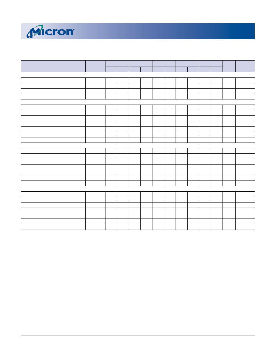
ELECTRICAL CHARACTERISTICS AND RECOMMENDED AC OPERATING CONDITIONS
(Note 1) (0°C
≤ T
A ≤ +70°C; VDD = +3.3V +0.3V/-0.165V unless otherwise noted)
-4.4
-5
-6
-7.5
-10
DESCRIPTION
SYMBOL MIN MAX MIN MAX MIN MAX MIN MAX MIN MAX UNITS
NOTES
Clock
Clock cycle time
tKC
4.4
5.0
6.0
7.5
10
ns
Clock frequency
fKF
225
200
166
133
100
MHz
Clock HIGH time
tKH
1.7
2.0
2.3
2.5
3.0
ns
2
Clock LOW time
tKL
1.7
2.0
2.3
2.5
3.0
ns
2
Output Times
Clock to output valid
tKQ
2.6
2.8
3.5
4.0
5.0
ns
Clock to output invalid
tKQX
1
1.0
1.5
ns
3
Clock to output in Low-Z
tKQLZ
0
1.5
ns
3, 4, 5, 6
Clock to output in High-Z
tKQHZ
2.6
2.8
3.5
4.2
5.0
ns
3, 4, 5, 6
OE# to output valid
tOEQ
2.6
2.8
3.5
4.2
5.0
ns
7
OE# to output in Low-Z
tOELZ
0
ns
3, 4, 5, 6
OE# to output in High-Z
tOEHZ
2.6
2.8
3.5
4.2
4.5
ns
3, 4, 5, 6
Setup Times
Address
tAS
1
1.3
1.5
2.0
ns
8, 9
Address status (ADSC#, ADSP#)
tADSS
1
1.3
1.5
2.0
ns
8, 9
Address advance (ADV#)
tAAS
1
1.3
1.5
2.0
ns
8, 9
Write signals
tWS
1
1.3
1.5
2.0
ns
8, 9
(BWa#-BWd#, BWE#, GW#)
Data-in
tDS
1
1.3
1.5
2.0
ns
8, 9
Chip enables (CE#, CE2#, CE2)
tCES
1
1.3
1.5
2.0
ns
8, 9
Hold Times
Address
tAH
0.3
0.5
ns
8, 9
Address status (ADSC#, ADSP#)
tADSH
0.3
0.5
ns
8, 9
Address advance (ADV#)
tAAH
0.3
0.5
ns
8, 9
Write signals
tWH
0.3
0.5
ns
8, 9
(BWa#-BWd#, BWE#, GW#)
Data-in
tDH
0.3
0.5
ns
8, 9
Chip enables (CE#, CE2#, CE2)
tCEH
0.3
0.5
ns
8, 9
相關(guān)PDF資料 |
PDF描述 |
|---|---|
| MT58L512Y36FT-8.5 | 512K X 36 CACHE SRAM, 8.5 ns, PQFP100 |
| MT58V1MV18DT-10 | 1M X 18 CACHE SRAM, 5 ns, PQFP100 |
| MT5C2565EC-70/IT | 64K X 4 STANDARD SRAM, 70 ns, CQCC28 |
| MT5C256K16B2DJ-12PAT | 256K X 16 STANDARD SRAM, 12 ns, PDSO54 |
| MT5C256K16B2DJ-35LAT | 256K X 16 STANDARD SRAM, 35 ns, PDSO54 |
相關(guān)代理商/技術(shù)參數(shù) |
參數(shù)描述 |
|---|---|
| MT58L128L36P1T-5 TR | 制造商:Cypress Semiconductor 功能描述:128KX36 SRAM PLASTIC BGA 3.3V |
| MT58L128L36P1T-6 | 制造商:Cypress Semiconductor 功能描述:128KX36 SRAM PLASTIC TQFP 3.3V |
| MT58L128L36P1T-6 TR | 制造商:Cypress Semiconductor 功能描述:128KX36 SRAM PLASTIC TQFP 3.3V |
| MT58L128L36P1T-7.5 | 制造商:Cypress Semiconductor 功能描述:SRAM Chip Sync Quad 3.3V 4M-Bit 128K x 36 4ns 100-Pin TQFP 制造商:Rochester Electronics LLC 功能描述:- Bulk 制造商:Micron Technology Inc 功能描述:128K X 36 CACHE SRAM, 4 ns, PQFP100 |
| MT58L128L36P1T-7.5 IT | 制造商:Cypress Semiconductor 功能描述:128KX36 SRAM PLASTIC IND TEMP |
發(fā)布緊急采購,3分鐘左右您將得到回復(fù)。