- 您現(xiàn)在的位置:買賣IC網(wǎng) > PDF目錄296642 > MT58L128L36P1T-5 (CYPRESS SEMICONDUCTOR CORP) 128K X 36 CACHE SRAM, 2.8 ns, PQFP100 PDF資料下載
參數(shù)資料
| 型號: | MT58L128L36P1T-5 |
| 廠商: | CYPRESS SEMICONDUCTOR CORP |
| 元件分類: | SRAM |
| 英文描述: | 128K X 36 CACHE SRAM, 2.8 ns, PQFP100 |
| 封裝: | PLASTIC, MS-026, TQFP-100 |
| 文件頁數(shù): | 1/30頁 |
| 文件大小: | 481K |
| 代理商: | MT58L128L36P1T-5 |
當(dāng)前第1頁第2頁第3頁第4頁第5頁第6頁第7頁第8頁第9頁第10頁第11頁第12頁第13頁第14頁第15頁第16頁第17頁第18頁第19頁第20頁第21頁第22頁第23頁第24頁第25頁第26頁第27頁第28頁第29頁第30頁
1
4Mb: 256K x 18, 128K x 32/36 Pipelined, SCD SyncBurst SRAM
2003, Micron Technology, Inc.
MT58L256L18P1_F.p65 – Rev. F, Pub. 1/03 EN
4Mb: 256K x 18, 128K x 32/36
PIPELINED, SCD SYNCBURST SRAM
PRODUCTS AND SPECIFICATIONS DISCUSSED HEREIN ARE SUBJECT TO CHANGE BY MICRON WITHOUT NOTICE.
FEATURES
Fast clock and OE# access times
Single +3.3V +0.3V/-0.165V power supply (VDD)
Separate +3.3V or +2.5V isolated output buffer
supply (VDDQ)
SNOOZE MODE for reduced-power standby
Single-cycle deselect (Pentium BSRAM-compatible)
Common data inputs and data outputs
Individual BYTE WRITE control and GLOBAL WRITE
Three chip enables for simple depth expansion
and address pipelining
Clock-controlled and registered addresses, data
I/Os and control signals
Internally self-timed WRITE cycle
Burst control pin (interleaved or linear burst)
Automatic power-down for portable applications
165-pin FBGA package
100-pin TQFP package
Low capacitive bus loading
x18, x32, and x36 versions available
OPTIONS
MARKING
Timing (Access/Cycle/MHz)
2.6ns/4.4ns/225 MHz
-4.4
2.8ns/5ns/200 MHz
-5
3.5ns/6ns/166 MHz
-6
4.0ns/7.5ns/133 MHz
-7.5
5ns/10ns/100 MHz
-10
Configurations
3.3V I/O
256K x 18
MT58L256L18P1
128K x 32
MT58L128L32P1
128K x 36
MT58L128L36P1
2.5V I/O
256K x 18
MT58L256V18P1
128K x 32
MT58L128V32P1
128K x 36
MT58L128V36P1
Packages
100-pin TQFP
T
165-pin FBGA
F*
Operating Temperature Range
Commercial (0°C to +70°C)
None
Industrial (-40°C to +85°C)**
IT
Part Number Example:
MT58L256L18P1T-6
MT58L256L18P1, MT58L128L32P1,
MT58L128L36P1; MT58L256V18P1,
MT58L128V32P1, MT58L128V36P1
3.3V VDD, 3.3V or 2.5V I/O, Pipelined, Single-Cycle
Deselect
4Mb SYNCBURST
SRAM
* A Part Marking Guide for the FBGA devices can be found on Micron’s
Web site—http://www.micron.com/support/index.html. The 165-ball
** Industrial temperature range offered in specific speed grades and
configurations. Contact factory for more information.
GENERAL DESCRIPTION
The Micron SyncBurst SRAM family employs
high-speed, low-power CMOS designs that are fabri-
cated using an advanced CMOS process.
Micron’s 4Mb SyncBurst SRAMs integrate a
256K x 18, 128K x 32, or 128K x 36 SRAM core with ad-
vanced synchronous peripheral circuitry and a 2-bit
burst counter. All synchronous inputs pass through
registers controlled by a positive-edge-triggered single
clock input (CLK). The synchronous inputs include all
addresses, all data inputs, active LOW chip enable
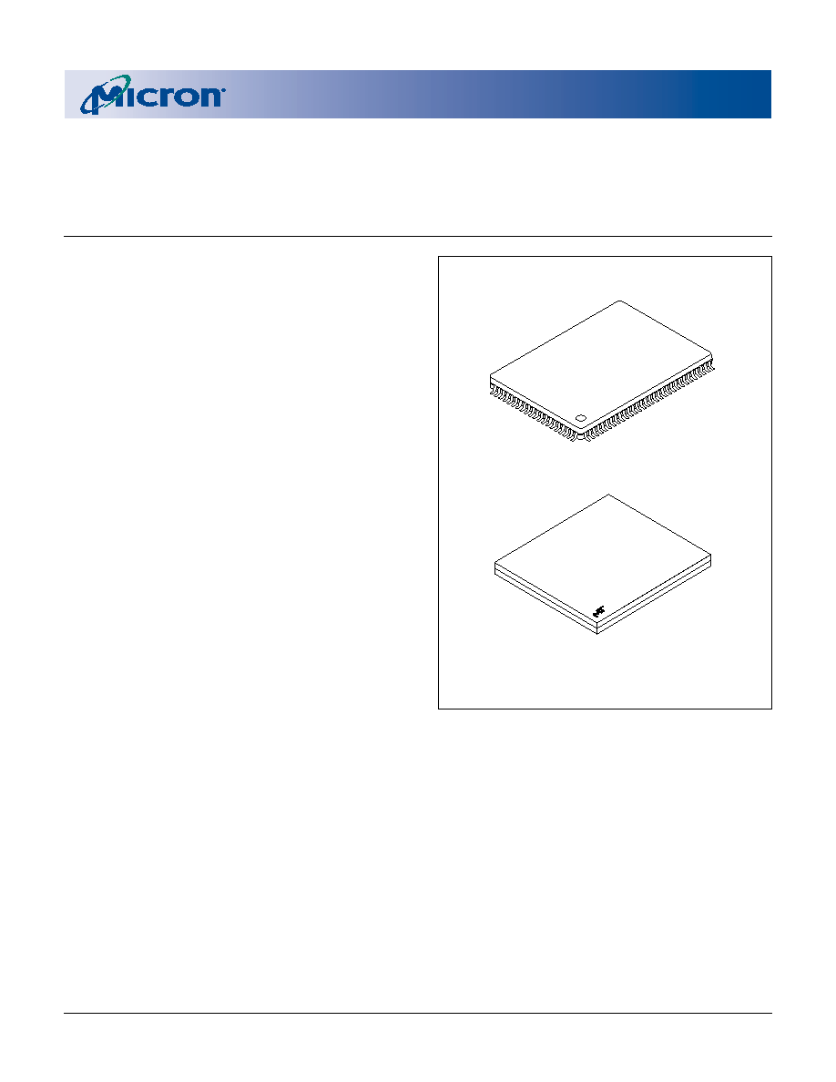
NOTE: 1. JEDEC-standard MS-026 BHA (LQFP).
2. The 165-ball FBGA is not recommended for new
designs in the 4Mb density.
100-PIN TQFP1
165-BALL FBGA2
相關(guān)PDF資料 |
PDF描述 |
|---|---|
| MT58L512Y36FT-8.5 | 512K X 36 CACHE SRAM, 8.5 ns, PQFP100 |
| MT58V1MV18DT-10 | 1M X 18 CACHE SRAM, 5 ns, PQFP100 |
| MT5C2565EC-70/IT | 64K X 4 STANDARD SRAM, 70 ns, CQCC28 |
| MT5C256K16B2DJ-12PAT | 256K X 16 STANDARD SRAM, 12 ns, PDSO54 |
| MT5C256K16B2DJ-35LAT | 256K X 16 STANDARD SRAM, 35 ns, PDSO54 |
相關(guān)代理商/技術(shù)參數(shù) |
參數(shù)描述 |
|---|---|
| MT58L128L36P1T-5 TR | 制造商:Cypress Semiconductor 功能描述:128KX36 SRAM PLASTIC BGA 3.3V |
| MT58L128L36P1T-6 | 制造商:Cypress Semiconductor 功能描述:128KX36 SRAM PLASTIC TQFP 3.3V |
| MT58L128L36P1T-6 TR | 制造商:Cypress Semiconductor 功能描述:128KX36 SRAM PLASTIC TQFP 3.3V |
| MT58L128L36P1T-7.5 | 制造商:Cypress Semiconductor 功能描述:SRAM Chip Sync Quad 3.3V 4M-Bit 128K x 36 4ns 100-Pin TQFP 制造商:Rochester Electronics LLC 功能描述:- Bulk 制造商:Micron Technology Inc 功能描述:128K X 36 CACHE SRAM, 4 ns, PQFP100 |
| MT58L128L36P1T-7.5 IT | 制造商:Cypress Semiconductor 功能描述:128KX36 SRAM PLASTIC IND TEMP |
發(fā)布緊急采購,3分鐘左右您將得到回復(fù)。