- 您現(xiàn)在的位置:買賣IC網(wǎng) > PDF目錄296642 > MT48LC8M8A2TG-8EL:GIT 8M X 8 SYNCHRONOUS DRAM, 6 ns, PDSO54 PDF資料下載
參數(shù)資料
| 型號(hào): | MT48LC8M8A2TG-8EL:GIT |
| 元件分類: | DRAM |
| 英文描述: | 8M X 8 SYNCHRONOUS DRAM, 6 ns, PDSO54 |
| 封裝: | 0.400 INCH, PLASTIC, TSOP2-54 |
| 文件頁數(shù): | 2/55頁 |
| 文件大小: | 1454K |
第1頁當(dāng)前第2頁第3頁第4頁第5頁第6頁第7頁第8頁第9頁第10頁第11頁第12頁第13頁第14頁第15頁第16頁第17頁第18頁第19頁第20頁第21頁第22頁第23頁第24頁第25頁第26頁第27頁第28頁第29頁第30頁第31頁第32頁第33頁第34頁第35頁第36頁第37頁第38頁第39頁第40頁第41頁第42頁第43頁第44頁第45頁第46頁第47頁第48頁第49頁第50頁第51頁第52頁第53頁第54頁第55頁
10
64Mb: x4, x8, x16 SDRAM
Micron Technology, Inc., reserves the right to change products or specifications without notice.
64MSDRAM.pmd – Rev. H; Pub. 12/04
2002 Micron Technology, Inc. All rights reserved.
64Mb: x4, x8, x16
SDRAM
ALLOWABLE OPERATING
FREQUENCY (MHz)
CAS
SPEED
LATENCY = 2
LATENCY = 3
-6
–
≤ 166
-7E
≤ 133
≤ 143
-75
≤ 100
≤ 133
-8E
≤ 100
≤ 125
Operating Mode
The normal operating mode is selected by setting
M7 and M8 to zero; the other combinations of values for
M7 and M8 are reserved for future use and/or test
modes. The programmed burst length applies to both
READ and WRITE bursts.
Test modes and reserved states should not be used
because unknown operation or incompatibility with
future versions may result.
Write Burst Mode
When M9 = 0, the burst length programmed via
M0-M2 applies to both READ and WRITE bursts; when
M9 = 1, the programmed burst length applies to
READ bursts, but write accesses are single-location
(nonburst) accesses.
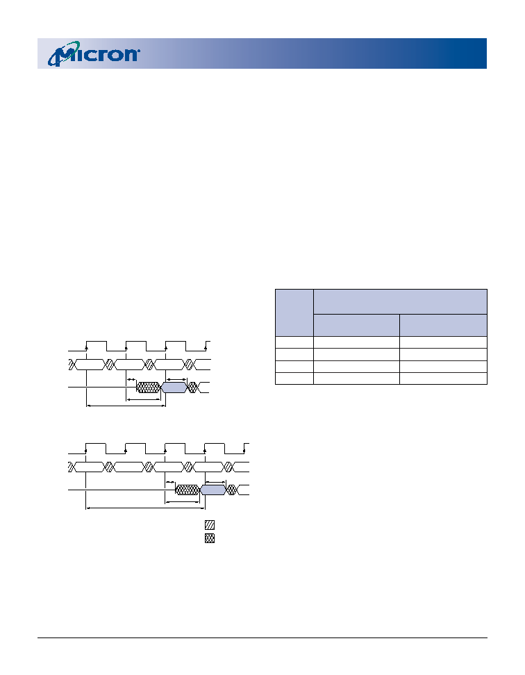
CAS Latency
The CAS latency is the delay, in clock cycles, be-
tween the registration of a READ command and the
availability of the first piece of output data. The la-
tency can be set to two or three clocks.
If a READ command is registered at clock edge n,
and the latency is m clocks, the data will be available by
clock edge n + m. The DQs will start driving as a result of
the clock edge one cycle earlier (n + m - 1), and provided
that the relevant access times are met, the data will be
valid by clock edge n + m. For example, assuming that
the clock cycle time is such that all relevant access times
are met, if a READ command is registered at T0 and the
latency is programmed to two clocks, the DQs will start
driving after T1 and the data will be valid by T2, as
shown in Figure 2. Table 2 indicates the operating fre-
quencies at which each CAS latency setting can be used.
Reserved states should not be used as unknown
operation or incompatibility with future versions
may result.
Figure 2
CAS Latency
CLK
DQ
T2
T1
T3
T0
CAS Latency = 3
LZ
DOUT
tOH
t
COMMAND
NOP
READ
tAC
NOP
T4
NOP
DON’T CARE
UNDEFINED
CLK
DQ
T2
T1
T3
T0
CAS Latency = 2
LZ
DOUT
tOH
t
COMMAND
NOP
READ
tAC
NOP
Table 2
CAS Latency
相關(guān)PDF資料 |
PDF描述 |
|---|---|
| MT4JSF6464HIY-80BXX | 64M X 64 DDR DRAM MODULE, ZMA204 |
| MT4JSF6464HY-1G4XX | 64M X 64 DDR DRAM MODULE, ZMA204 |
| MT4LC16M4A7DJ-6S | 16M X 4 FAST PAGE DRAM, 60 ns, PDSO32 |
| MT58L128L36P1T-5 | 128K X 36 CACHE SRAM, 2.8 ns, PQFP100 |
| MT58L512Y36FT-8.5 | 512K X 36 CACHE SRAM, 8.5 ns, PQFP100 |
相關(guān)代理商/技術(shù)參數(shù) |
參數(shù)描述 |
|---|---|
| MT48LCM32B2P | 制造商:MICRON 制造商全稱:Micron Technology 功能描述:SDR SDRAM MT48LC2M32B2 a?? 512K x 32 x 4 Banks |
| MT48NN | 功能描述:插線板 48POS AUDIO PATCHBAY RoHS:否 制造商:Switchcraft 產(chǎn)品類型:Bantam (TT) 正規(guī)化: 高度/機(jī)架數(shù)量: 深度: 端接類型: 位置/觸點(diǎn)數(shù)量:48 |
| MT48NNX | 功能描述:插線板 48POS AUDIO PATCHBAY RoHS:否 制造商:Switchcraft 產(chǎn)品類型:Bantam (TT) 正規(guī)化: 高度/機(jī)架數(shù)量: 深度: 端接類型: 位置/觸點(diǎn)數(shù)量:48 |
| MT48NS | 功能描述:插線板 1 RU PANEL 48 LF JA RoHS:否 制造商:Switchcraft 產(chǎn)品類型:Bantam (TT) 正規(guī)化: 高度/機(jī)架數(shù)量: 深度: 端接類型: 位置/觸點(diǎn)數(shù)量:48 |
| MT48NSX | 功能描述:插線板 1/4" LF SLDR BAY 1RU, 2X24, NORM STR RoHS:否 制造商:Switchcraft 產(chǎn)品類型:Bantam (TT) 正規(guī)化: 高度/機(jī)架數(shù)量: 深度: 端接類型: 位置/觸點(diǎn)數(shù)量:48 |
發(fā)布緊急采購,3分鐘左右您將得到回復(fù)。