- 您現(xiàn)在的位置:買賣IC網(wǎng) > PDF目錄296642 > MT48LC4M32LFB5-10ES:G 4M X 32 SYNCHRONOUS DRAM, 7 ns, PBGA90 PDF資料下載
參數(shù)資料
| 型號: | MT48LC4M32LFB5-10ES:G |
| 元件分類: | DRAM |
| 英文描述: | 4M X 32 SYNCHRONOUS DRAM, 7 ns, PBGA90 |
| 封裝: | 8 X 13 MM, LEAD FREE, VFBGA-90 |
| 文件頁數(shù): | 37/69頁 |
| 文件大小: | 6213K |
第1頁第2頁第3頁第4頁第5頁第6頁第7頁第8頁第9頁第10頁第11頁第12頁第13頁第14頁第15頁第16頁第17頁第18頁第19頁第20頁第21頁第22頁第23頁第24頁第25頁第26頁第27頁第28頁第29頁第30頁第31頁第32頁第33頁第34頁第35頁第36頁當(dāng)前第37頁第38頁第39頁第40頁第41頁第42頁第43頁第44頁第45頁第46頁第47頁第48頁第49頁第50頁第51頁第52頁第53頁第54頁第55頁第56頁第57頁第58頁第59頁第60頁第61頁第62頁第63頁第64頁第65頁第66頁第67頁第68頁第69頁
128Mb: x16, x32
MOBILE SDRAM
09005aef8071a76b
Micron Technology, Inc., reserves the right to change products or specifications without notice.
128Mbx16x32Mobile_2.fm - Rev. G (DRAFT) 7/04 EN
42
2001 Micron Technology, Inc. All rights reserved.
Absolute Maximum Ratings
Voltage on VDD/VDDQ Supply
Relative to VSS(LC devices) . . . . . . . . . . .-1V to +4.6V
Relative to VSS(V devices) . . . . . . . . . . . 0.5V to +3.6V
Voltage on Inputs, NC or I/O Pins
Relative to VSS(LC, devices) . . . . . . . . . .-1V to +4.6V
Relative to VSS(V devices) . . . . . . . . . . -0.5V to +3.6V
Operating Temperature
TA (Commercial) . . . . . . . . . . . . . . . . . . . 0°C to +70°C
TA (Industrial) . . . . . . . . . . . . . . . . . . . -40°C to +85°C
TA (Extended) . . . . . . . . . . . . . . . . . . . -25°C to +75°C
Storage Temperature (plastic) . . . . -55°C to +150°C
Stresses greater than those listed under “Absolute
Maximum Ratings” may cause permanent damage to
the device. This is a stress rating only, and functional
operation of the device at these or any other condi-
tions above those indicated in the operational sections
of this specification is not implied. Exposure to abso-
lute maximum rating conditions for extended periods
may affect reliability.
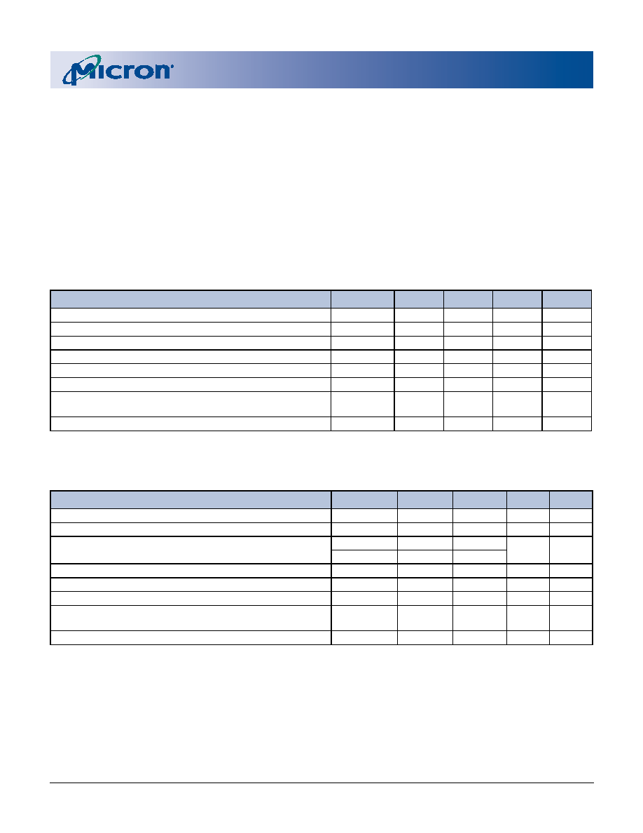
Table 12:
DC Electrical Characteristics and Operating Conditions (LC Version)
PARAMETER/CONDITION
SYMBOL
MIN
MAX
UNITS
NOTES
Supply Voltage
VDD
33.6
V
I/O Supply Voltage
VDDQ3
3.6
V
Input High Voltage: Logic 1; All inputs
VIH
2VDD + 0.3
V
Input Low Voltage: Logic 0; All inputs
VIL
-0.3
0.8
V
Data Output High Voltage: Logic 1; All inputs
VOH
2.4
–
V
Data Output LOW Voltage: Logic 0; All inputs
VOL
–0.4
V
Input Leakage Current:
Any Input 0V
≤ VIN ≤ VDD (All other pins not under test = 0V)
II
-5
5
A
Output Leakage Current: DQs are disabled; 0V
≤ VOUT ≤ VDDQ
IOZ
-5
5
A
Table 13:
DC Electrical Characteristics and Operating Conditions (V Version)
PARAMETER/CONDITION
SYMBOL
MIN
MAX
UNITS
NOTES
Supply Voltage
VDD
2.3
2.7
V
I/O Supply Voltage
VDDQ
1.65
2.7
V
Input High Voltage: Logic 1; All inputs
VIH (DQ)
1.25
VDDQ + 0.3
V
VIH (non-DQ)
1.25
VDD + 0.3
Input Low Voltage: Logic 0; All inputs
VIL
-0.3
+0.55
V
Data Output High Voltage: Logic 1; All inputs
VOH
VDDQ - 0.2
–
V
Data Output Low Voltage: Logic 0; All inputs
VOL
–0.2
V
Input Leakage Current:
Any input 0V
≤ VIN ≤ VDD (All other pins not under test = 0V)
II
-5
5
A
Output Leakage Current: DQs are disabled; 0V
≤ VOUT ≤ VDDQ
IOZ
-5
5
A
相關(guān)PDF資料 |
PDF描述 |
|---|---|
| MT48V4M32TG-8XT | 4M X 32 SYNCHRONOUS DRAM, 7 ns, PDSO54 |
| MT48LC8M8A2TG-8EL:GIT | 8M X 8 SYNCHRONOUS DRAM, 6 ns, PDSO54 |
| MT4JSF6464HIY-80BXX | 64M X 64 DDR DRAM MODULE, ZMA204 |
| MT4JSF6464HY-1G4XX | 64M X 64 DDR DRAM MODULE, ZMA204 |
| MT4LC16M4A7DJ-6S | 16M X 4 FAST PAGE DRAM, 60 ns, PDSO32 |
相關(guān)代理商/技術(shù)參數(shù) |
參數(shù)描述 |
|---|
發(fā)布緊急采購,3分鐘左右您將得到回復(fù)。