- 您現(xiàn)在的位置:買賣IC網(wǎng) > PDF目錄296642 > MT48LC4M32LFB5-10ES:G 4M X 32 SYNCHRONOUS DRAM, 7 ns, PBGA90 PDF資料下載
參數(shù)資料
| 型號(hào): | MT48LC4M32LFB5-10ES:G |
| 元件分類: | DRAM |
| 英文描述: | 4M X 32 SYNCHRONOUS DRAM, 7 ns, PBGA90 |
| 封裝: | 8 X 13 MM, LEAD FREE, VFBGA-90 |
| 文件頁(yè)數(shù): | 20/69頁(yè) |
| 文件大小: | 6213K |
第1頁(yè)第2頁(yè)第3頁(yè)第4頁(yè)第5頁(yè)第6頁(yè)第7頁(yè)第8頁(yè)第9頁(yè)第10頁(yè)第11頁(yè)第12頁(yè)第13頁(yè)第14頁(yè)第15頁(yè)第16頁(yè)第17頁(yè)第18頁(yè)第19頁(yè)當(dāng)前第20頁(yè)第21頁(yè)第22頁(yè)第23頁(yè)第24頁(yè)第25頁(yè)第26頁(yè)第27頁(yè)第28頁(yè)第29頁(yè)第30頁(yè)第31頁(yè)第32頁(yè)第33頁(yè)第34頁(yè)第35頁(yè)第36頁(yè)第37頁(yè)第38頁(yè)第39頁(yè)第40頁(yè)第41頁(yè)第42頁(yè)第43頁(yè)第44頁(yè)第45頁(yè)第46頁(yè)第47頁(yè)第48頁(yè)第49頁(yè)第50頁(yè)第51頁(yè)第52頁(yè)第53頁(yè)第54頁(yè)第55頁(yè)第56頁(yè)第57頁(yè)第58頁(yè)第59頁(yè)第60頁(yè)第61頁(yè)第62頁(yè)第63頁(yè)第64頁(yè)第65頁(yè)第66頁(yè)第67頁(yè)第68頁(yè)第69頁(yè)
128Mb: x16, x32
MOBILE SDRAM
09005aef8071a76b
Micron Technology, Inc., reserves the right to change products or specifications without notice.
128Mbx16x32Mobile_2.fm - Rev. G (DRAFT) 7/04 EN
27
2001 Micron Technology, Inc. All rights reserved.
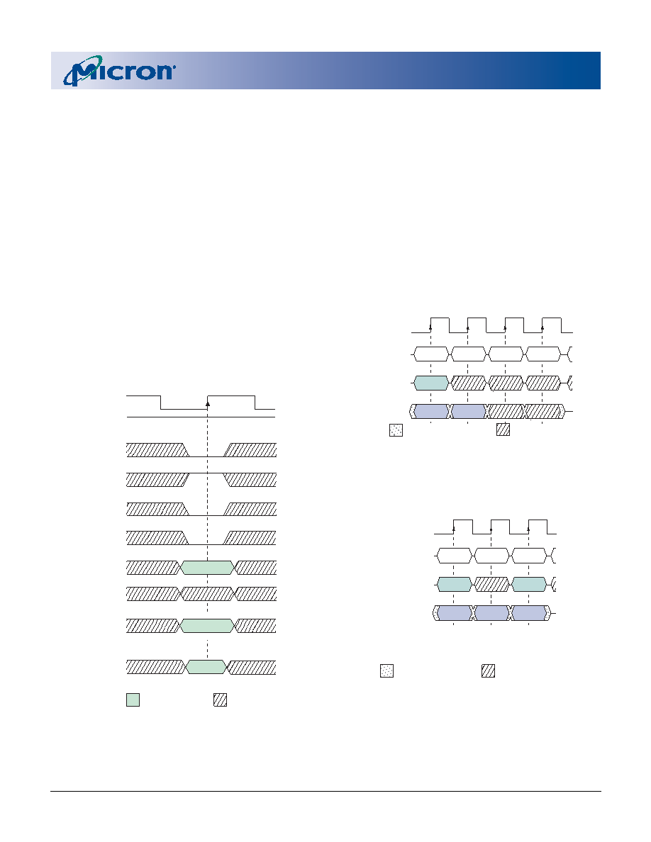
WRITEs
WRITE bursts are initiated with a WRITE command,
as shown in Figure 20.
The starting column and bank addresses are pro-
vided with the WRITE command, and auto precharge
is either enabled or disabled for that access. If auto
precharge is enabled, the row being accessed is pre-
charged at the completion of the burst. For the WRITE
commands used in the following illustrations, auto
precharge is disabled.
During WRITE bursts, the first valid data-in element
will be registered coincident with the WRITE com-
mand. Subsequent data elements will be registered on
each successive positive clock edge. Upon completion
of a fixed-length burst, assuming no other commands
have been initiated, the DQs will remain High-Z and
any additional input data will be ignored (see
Figure 21). A full-page burst will continue until termi-
nated. (At the end of the page, it will wrap to column 0
and continue.)
Figure 20: WRITE Command
Data for any WRITE burst may be truncated with a
subsequent WRITE command, and data for a fixed-
length WRITE burst may be immediately followed by
data for a WRITE command. The new WRITE com-
mand can be issued on any clock following the previ-
ous WRITE command, and the data provided
coincident with the new command applies to the new
command. An example is shown in Figure 21. Data n +
1 is either the last of a burst of two or the last desired of
a longer burst. The 128Mb SDRAM uses a pipelined
architecture and therefore does not require the 2n rule
associated with a prefetch architecture. A WRITE com-
mand can be initiated on any clock cycle following a
previous WRITE command. Full-speed random write
accesses within a page can be performed to the same
bank, as shown in Figure 22, or each subsequent
WRITE may be performed to a different bank.
Figure 21: WRITE Burst
Figure 22: WRITE to WRITE
Data for any WRITE burst may be truncated with a
subsequent READ command, and data for a fixed-
length WRITE burst may be immediately followed by a
READ command. Once the READ command is regis-
tered, the data inputs will be ignored, and writes will
CS#
WE#
CAS#
RAS#
CKE
CLK
COLUMN
ADDRESS
DON’T CARE
HIGH
ENABLE AUTO PRECHARGE
DISABLE AUTO PRECHARGE
BANK
ADDRESS
x16: A0-A8
x32: A0-A7
A10
BA0,1
A9, A11
VALID ADDRESS
CLK
DQ
DIN
n
T2
T1
T3
T0
COMMAND
ADDRESS
NOP
WRITE
DIN
n + 1
NOP
BANK,
COL n
NOTE:
Burst length = 2. DQM is LOW.
DON’T CARE
TRANSITIONING DATA
DON’T CARE
CLK
DQ
T2
T1
T0
COMMAND
ADDRESS
NOP
WRITE
BANK,
COL n
BANK,
COL b
DIN
n
DIN
n + 1
DIN
b
NOTE:
DQM is LOW. Each WRITE
command may be to any bank.
TRANSITIONING DATA
相關(guān)PDF資料 |
PDF描述 |
|---|---|
| MT48V4M32TG-8XT | 4M X 32 SYNCHRONOUS DRAM, 7 ns, PDSO54 |
| MT48LC8M8A2TG-8EL:GIT | 8M X 8 SYNCHRONOUS DRAM, 6 ns, PDSO54 |
| MT4JSF6464HIY-80BXX | 64M X 64 DDR DRAM MODULE, ZMA204 |
| MT4JSF6464HY-1G4XX | 64M X 64 DDR DRAM MODULE, ZMA204 |
| MT4LC16M4A7DJ-6S | 16M X 4 FAST PAGE DRAM, 60 ns, PDSO32 |
相關(guān)代理商/技術(shù)參數(shù) |
參數(shù)描述 |
|---|
發(fā)布緊急采購(gòu),3分鐘左右您將得到回復(fù)。