- 您現(xiàn)在的位置:買賣IC網(wǎng) > PDF目錄296642 > MT46V64M4TG-75E 64M X 4 DDR DRAM, 0.75 ns, PDSO66 PDF資料下載
參數(shù)資料
| 型號: | MT46V64M4TG-75E |
| 元件分類: | DRAM |
| 英文描述: | 64M X 4 DDR DRAM, 0.75 ns, PDSO66 |
| 封裝: | 0.400 INCH, PLASTIC, TSOP-66 |
| 文件頁數(shù): | 55/83頁 |
| 文件大小: | 2343K |
| 代理商: | MT46V64M4TG-75E |
第1頁第2頁第3頁第4頁第5頁第6頁第7頁第8頁第9頁第10頁第11頁第12頁第13頁第14頁第15頁第16頁第17頁第18頁第19頁第20頁第21頁第22頁第23頁第24頁第25頁第26頁第27頁第28頁第29頁第30頁第31頁第32頁第33頁第34頁第35頁第36頁第37頁第38頁第39頁第40頁第41頁第42頁第43頁第44頁第45頁第46頁第47頁第48頁第49頁第50頁第51頁第52頁第53頁第54頁當(dāng)前第55頁第56頁第57頁第58頁第59頁第60頁第61頁第62頁第63頁第64頁第65頁第66頁第67頁第68頁第69頁第70頁第71頁第72頁第73頁第74頁第75頁第76頁第77頁第78頁第79頁第80頁第81頁第82頁第83頁
256Mb: x4, x8, x16
DDR SDRAM
09005aef8076894f
Micron Technology, Inc., reserves the right to change products or specifications without notice.
256MBDDRx4x8x16_2.fm - Rev. K 9/04 EN
59
2003 Micron Technology, Inc. All rights reserved.
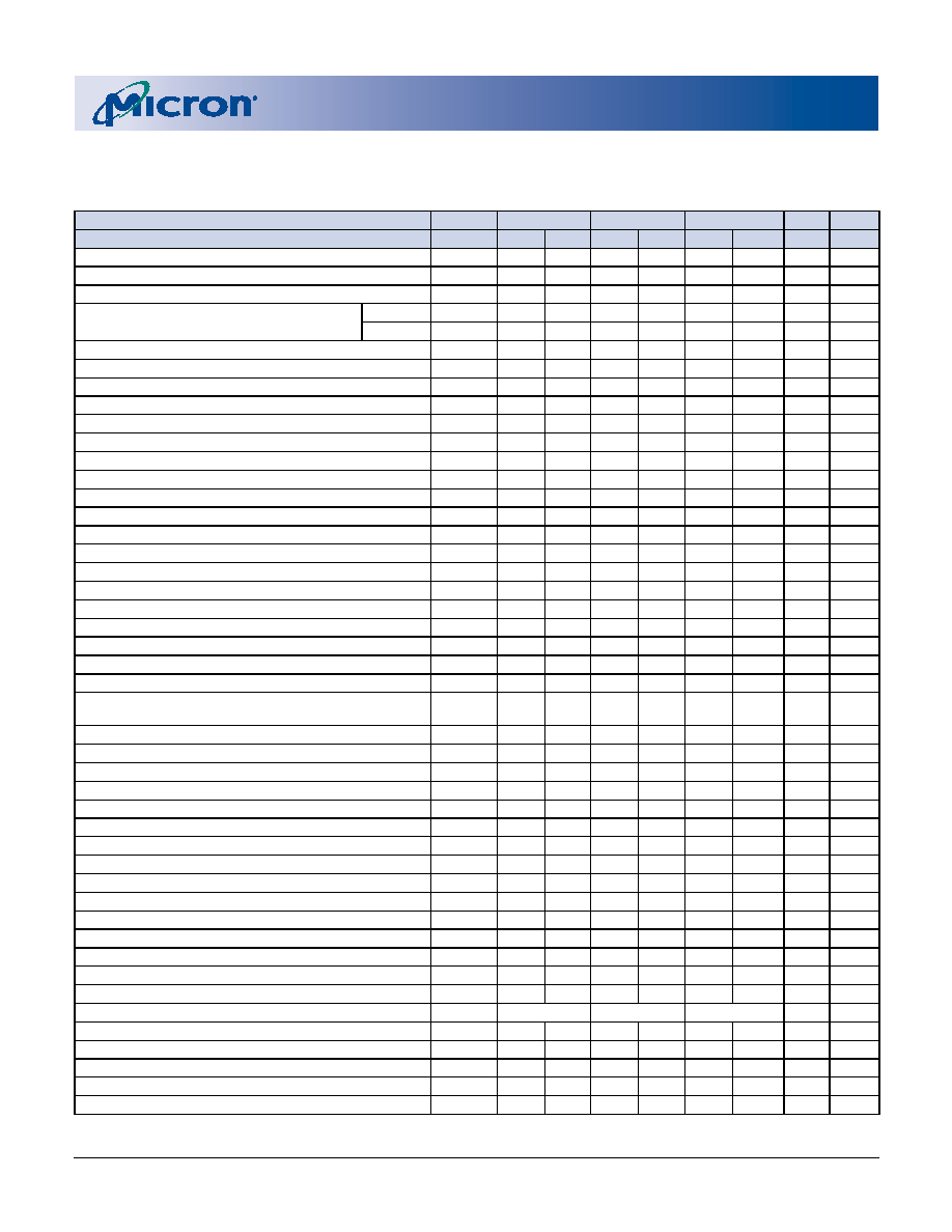
Table 26:
Electrical Characteristics and Recommended AC Operating Conditions
(-6/-6T/-75E)
Notes: 1–5, 14–17, 33; notes appear on pages 62–65; 0°C
≤ T
A ≤ +70°C; VDDQ = +2.5V ±0.2V, VDD = +2.5V ±0.2V
AC CHARACTERISTICS
-6 (FBGA)
-6T (TSOP)
-75E
PARAMETER
SYMBOL
MIN
MAX
MIN
MAX
MIN
MAX UNITS NOTES
Access window of DQs from CK/CK#
tAC
-0.70
+0.70
-0.70
+0.70
-0.75
+0.75
ns
CK high-level width
tCH
0.45
0.55
0.45
0.55
0.45
0.55
tCK
30
CK low-level width
tCL
0.45
0.55
0.45
0.55
0.45
0.55
tCK
30
Clock cycle time
CL = 2.5
tCK (2.5)
6
13
6
13
7.5
13
ns
45, 51
CL = 2
tCK (2)
7.5
13
7.5
13
7.5
13
ns
45, 51
DQ and DM input hold time relative to DQS
tDH
0.45
0.5
ns
26, 31
DQ and DM input setup time relative to DQS
tDS
0.45
0.5
ns
26, 31
DQ and DM input pulse width (for each input)
tDIPW
1.75
ns
31
Access window of DQS from CK/CK#
tDQSCK
-0.6
+0.6
-0.6
+0.6
-0.75
+0.75
ns
DQS input high pulse width
tDQSH
0.35
tCK
DQS input low pulse width
tDQSL
0.35
tCK
DQS–DQ skew, DQS to last DQ valid, per group, per access
tDQSQ
0.4
0.45
0.5
ns
25, 26
WRITE command to first DQS latching transition
tDQSS
0.75
1.25
0.75
1.25
0.75
1.25
tCK
DQS falling edge to CK rising – setup time
tDSS
0.2
tCK
DQS falling edge from CK rising – hold time
tDSH
0.2
tCK
Half clock period
tHP
tCH,tCL
ns
34
Data-out high-impedance window from CK/CK#
tHZ
+0.7
+0.75
ns
18, 42
Data-out low-impedance window from CK/CK#
tLZ
-0.7
-0.75
ns
18, 42
Address and control input hold time (fast slew rate)
tIH
F
0.75
0.90
ns
Address and control input setup time (fast slew rate)
tIS
F
0.75
0.90
ns
Address and control input hold time (slow slew rate)
tIH
S
0.8
1
ns
14
Address and control input setup time (slow slew rate)
tIS
S
0.8
1
ns
14
Address and Control input pulse width (for each input)
tIPW
2.2
ns
LOAD MODE REGISTER command cycle time
tMRD
12
15
ns
DQ–DQS hold, DQS to first DQ to go non-valid, per access
tQH
tHP
-tQHS
tHP
-tQHS
tHP
-tQHS
ns
25, 26
Data hold skew factor
tQHS
0.5
0.55
0.75
ns
ACTIVE to PRECHARGE command
tRAS
42
70,000
42
70,000
40
120,000
ns
35, 53
ACTIVE to READ with auto precharge command
tRAP
15
ns
ACTIVE to ACTIVE/AUTO REFRESH command period
tRC
60
ns
AUTO REFRESH command period
tRFC
72
75
ns
49
ACTIVE to READ or WRITE delay
tRCD
15
ns
PRECHARGE command period
tRP
15
ns
DQS read preamble
tRPRE
0.9
1.1
0.9
1.1
0.9
1.1
tCK
43
DQS read postamble
tRPST
0.4
0.6
0.4
0.6
0.4
0.6
tCK
43
ACTIVE bank a to ACTIVE bank b command
tRRD
12
15
ns
DQS write preamble
tWPRE
0.25
tCK
DQS write preamble setup time
tWPRES
0
ns
20, 21
DQS write postamble
tWPST
0.4
0.6
0.4
0.6
0.4
0.6
tCK
19
Write recovery time
tWR
15
ns
Internal WRITE to READ command delay
tWTR
1
tCK
Data valid output window (DVW)
N/A
tQH - tDQSQ
ns
25
REFRESH to REFRESH command interval
tREFC
70.3
s
23
Average periodic refresh interval
tREFI
7.8
s
23
Terminating voltage delay to VDD
tVTD
0
ns
Exit SELF REFRESH to non-READ command
tXSNR
75
ns
Exit SELF REFRESH to READ command
tXSRD
200
tCK
相關(guān)PDF資料 |
PDF描述 |
|---|---|
| MT46V64M4FG-75Z | 64M X 4 DDR DRAM, 0.75 ns, PBGA60 |
| MT47H128M8HQ-3AT | 128M X 8 DDR DRAM, 0.4 ns, PBGA60 |
| MT47H64M16HR-3IT | 64M X 16 DDR DRAM, 0.4 ns, PBGA84 |
| MT48H8M16LFB4-8IT:JTR | 8M X 16 SYNCHRONOUS DRAM, 6 ns, PBGA54 |
| MT48LC4M32TG-10 | 4M X 32 SYNCHRONOUS DRAM, 7 ns, PDSO54 |
相關(guān)代理商/技術(shù)參數(shù) |
參數(shù)描述 |
|---|---|
| MT46V64M4TG-75Z | 制造商:MICRON 制造商全稱:Micron Technology 功能描述:DOUBLE DATA RATE DDR SDRAM |
| MT46V64M8 | 制造商:MICRON 制造商全稱:Micron Technology 功能描述:512Mb: x4, x8, x16 Double Data Rate SDRAM Features |
發(fā)布緊急采購,3分鐘左右您將得到回復(fù)。