- 您現(xiàn)在的位置:買賣IC網(wǎng) > PDF目錄296642 > MT46V64M4FG-75Z 64M X 4 DDR DRAM, 0.75 ns, PBGA60 PDF資料下載
參數(shù)資料
| 型號(hào): | MT46V64M4FG-75Z |
| 元件分類: | DRAM |
| 英文描述: | 64M X 4 DDR DRAM, 0.75 ns, PBGA60 |
| 封裝: | 8 X 14 MM, PLASTIC, FBGA-60 |
| 文件頁數(shù): | 60/83頁 |
| 文件大小: | 2343K |
| 代理商: | MT46V64M4FG-75Z |
第1頁第2頁第3頁第4頁第5頁第6頁第7頁第8頁第9頁第10頁第11頁第12頁第13頁第14頁第15頁第16頁第17頁第18頁第19頁第20頁第21頁第22頁第23頁第24頁第25頁第26頁第27頁第28頁第29頁第30頁第31頁第32頁第33頁第34頁第35頁第36頁第37頁第38頁第39頁第40頁第41頁第42頁第43頁第44頁第45頁第46頁第47頁第48頁第49頁第50頁第51頁第52頁第53頁第54頁第55頁第56頁第57頁第58頁第59頁當(dāng)前第60頁第61頁第62頁第63頁第64頁第65頁第66頁第67頁第68頁第69頁第70頁第71頁第72頁第73頁第74頁第75頁第76頁第77頁第78頁第79頁第80頁第81頁第82頁第83頁
256Mb: x4, x8, x16
DDR SDRAM
09005aef8076894f
Micron Technology, Inc., reserves the right to change products or specifications without notice.
256MBDDRx4x8x16_2.fm - Rev. K 9/04 EN
63
2003 Micron Technology, Inc. All rights reserved.
progress, DQS could be HIGH during this time,
depending on tDQSS.
22. t
RC (MIN) or tRFC (MIN) for IDD measurements
is the smallest multiple of tCK that meets the
minimum absolute value for the respective
parameter. tRAS (MAX) for IDD measurements is
the largest multiple of tCK that meets the maxi-
mum absolute value for tRAS.
23. The refresh period is 64ms. This equates to an
average refresh rate of 7.8125s. However, an
AUTO REFRESH command must be asserted at
least once every 70.3s; burst refreshing or post-
ing by the DRAM controller greater than eight
refresh cycles is not allowed.
24. The I/O capacitance per DQS and DQ byte/group
will not differ by more than this maximum
amount for any given device.
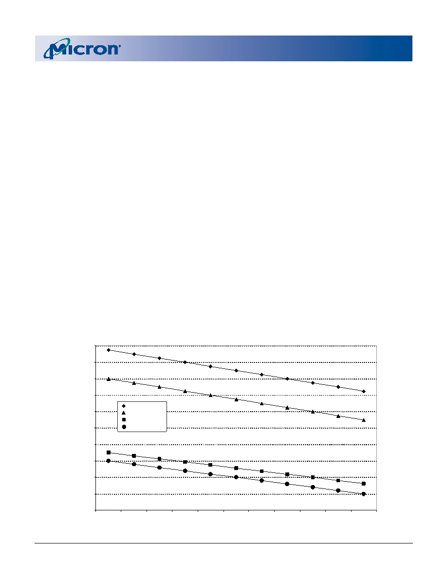
25.
The data valid window is derived by achieving
other specifications: tHP (tCK/2), tDQSQ, and
tQH (tQH = tHP - tQHS). The data valid window
derates in direct proportion to the clock duty
cycle and a practical data valid window can be
derived. The clock is allowed a maximum duty-
cycle variation of 45/55, because functionality
is uncertain when operating beyond a 45/55
ratio. Figure 35, Derating Data Valid Window
(tQH - tDQSQ), shows data valid window derat-
ing curves for duty cycles ranging between 50/
50 and 45/55.
26. Referenced to each output group: x4 = DQS with
DQ0–DQ3; x8 = DQS with DQ0–DQ7; x16 = LDQS
with DQ0–DQ7; and UDQS with DQ8–DQ15.
27. This limit is actually a nominal value and does not
result in a fail value. CKE is HIGH during
REFRESH command period (tRFC [MIN]) else
CKE is LOW (i.e., during standby).
28. To maintain a valid level, the transitioning edge of
the input must:
a.
Sustain a constant slew rate from the current
AC level through to the target AC level, VIL
(AC)
or VIH (AC).
b. Reach at least the target AC level.
c.
After the AC target level is reached, continue
to maintain at least the target DC level, VIL
(DC) or VIH (DC).
29. The Input capacitance per pin group will not dif-
fer by more than this maximum amount for any
given device.
30. CK and CK# input slew rate must be
≥ 1V/ns
(
≥ 2V/ns if measured differentially).
31. DQ and DM input slew rates must not deviate
from DQS by more than 10 percent. If the DQ/
DM/DQS slew rate is less than 0.5 V/ns, timing
must be derated: 50ps must be added to tDS and
3.750
3.700
3.650
3.600
3.550
3.500
3.450
3.400
3.350
3.300
3.250
3.400
3.350
3.300
3.250
3.200
3.150
3.100
3.050
3.000
2.950
2.900
2.500
2.463
2.425
2.388
2.350
2.313
2.275
2.238
2.200
2.163
2.125
1.8
2.0
2.2
2.4
2.6
2.8
3.0
3.2
3.4
3.6
3.8
50/50
49.5/50.5
49/51
48.5/52.5
48/52
47.5/53.5
47/53
46.5/54.5
46/54
45.5/55.5
45/55
Cl o ck Du ty C y c le
ns
—— -75 @ tCK = 10ns
—— -8 @ tCK = 10ns
—— -75 @ tCK = 7.5ns
—— -8 @ tCK = 8ns
Figure 35: Derating Data Valid Window (tQH - tDQSQ)
Examples are for speed grades through -75
相關(guān)PDF資料 |
PDF描述 |
|---|---|
| MT47H128M8HQ-3AT | 128M X 8 DDR DRAM, 0.4 ns, PBGA60 |
| MT47H64M16HR-3IT | 64M X 16 DDR DRAM, 0.4 ns, PBGA84 |
| MT48H8M16LFB4-8IT:JTR | 8M X 16 SYNCHRONOUS DRAM, 6 ns, PBGA54 |
| MT48LC4M32TG-10 | 4M X 32 SYNCHRONOUS DRAM, 7 ns, PDSO54 |
| MT48V8M16LFB4-8XT | 8M X 16 SYNCHRONOUS DRAM, 7 ns, PBGA54 |
相關(guān)代理商/技術(shù)參數(shù) |
參數(shù)描述 |
|---|---|
| MT46V64M4FJ-6 | 制造商:MICRON 制造商全稱:Micron Technology 功能描述:DOUBLE DATA RATE DDR SDRAM |
| MT46V64M4FJ-6T | 制造商:MICRON 制造商全稱:Micron Technology 功能描述:DOUBLE DATA RATE DDR SDRAM |
| MT46V64M4FJ-75Z | 制造商:MICRON 制造商全稱:Micron Technology 功能描述:DOUBLE DATA RATE DDR SDRAM |
發(fā)布緊急采購,3分鐘左右您將得到回復(fù)。