- 您現(xiàn)在的位置:買賣IC網(wǎng) > PDF目錄296642 > MT46V128M4P-75ZLIT:C 128M X 4 DDR DRAM, 0.75 ns, PDSO66 PDF資料下載
參數(shù)資料
| 型號(hào): | MT46V128M4P-75ZLIT:C |
| 元件分類: | DRAM |
| 英文描述: | 128M X 4 DDR DRAM, 0.75 ns, PDSO66 |
| 封裝: | 0.400 INCH, LEAD FREE, PLASTIC, TSOP-66 |
| 文件頁數(shù): | 73/94頁 |
| 文件大?。?/td> | 4179K |
第1頁第2頁第3頁第4頁第5頁第6頁第7頁第8頁第9頁第10頁第11頁第12頁第13頁第14頁第15頁第16頁第17頁第18頁第19頁第20頁第21頁第22頁第23頁第24頁第25頁第26頁第27頁第28頁第29頁第30頁第31頁第32頁第33頁第34頁第35頁第36頁第37頁第38頁第39頁第40頁第41頁第42頁第43頁第44頁第45頁第46頁第47頁第48頁第49頁第50頁第51頁第52頁第53頁第54頁第55頁第56頁第57頁第58頁第59頁第60頁第61頁第62頁第63頁第64頁第65頁第66頁第67頁第68頁第69頁第70頁第71頁第72頁當(dāng)前第73頁第74頁第75頁第76頁第77頁第78頁第79頁第80頁第81頁第82頁第83頁第84頁第85頁第86頁第87頁第88頁第89頁第90頁第91頁第92頁第93頁第94頁
09005aef80a1d9e7
Micron Technology, Inc., reserves the right to change products or specifications without notice.
512MBDDRx4x8x16_2.fm - Rev. J 1/06 EN
75
2000–2005 Micron Technology, Inc. All rights reserved.
512Mb: x4, x8, x16 DDR SDRAM
Notes
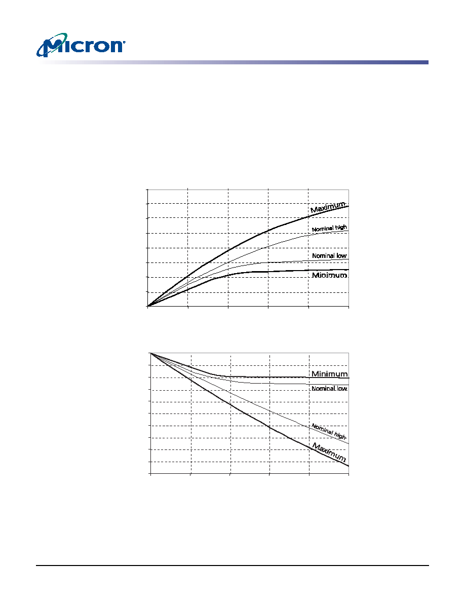
C. The full driver pull-up current variation from MIN to MAX process, temperature
and voltage will lie within the outer bounding lines of the V-I curve of Figure 39.
D. The driver pull-up current variation, within nominal voltage and temperature
limits, is expected, but not guaranteed, to lie within the inner bounding lines of
the V-I curve of Figure 39 on page 75.
E. The full ratio variation of the MAX to MIN pull-up and pull-down current should
be between 0.71 and 1.4 for device drain-to-source voltages from 0.1V to 1.0V at
the same voltage and temperature.
F. The full ratio variation of the nominal pull-up to pull-down current should be
unity ±10 percent, for device drain-to-source voltages from 0.1V to 1.0V.
Figure 38:
Reduced Drive Pull-Down Characteristics
Figure 39:
Reduced Drive Pull-Up Characteristics
39. The voltage levels used are derived from a minimum VDD level and the referenced test
load. In practice, the voltage levels obtained from a properly terminated bus will pro-
vide significantly different voltage values.
0
20
40
60
80
100
120
140
160
0.0
0.5
1.0
1.5
2.0
2.5
VOUT (V)
IOUT
(m
A
)
-200
-180
-160
-140
-120
-100
-80
-60
-40
-20
0
0.0
0.5
1.0
1.5
2.0
2.5
IOUT
(mA)
VDDQ - VOUT (V)
相關(guān)PDF資料 |
PDF描述 |
|---|---|
| MT46V64M4TG-75E | 64M X 4 DDR DRAM, 0.75 ns, PDSO66 |
| MT46V64M4FG-75Z | 64M X 4 DDR DRAM, 0.75 ns, PBGA60 |
| MT47H128M8HQ-3AT | 128M X 8 DDR DRAM, 0.4 ns, PBGA60 |
| MT47H64M16HR-3IT | 64M X 16 DDR DRAM, 0.4 ns, PBGA84 |
| MT48H8M16LFB4-8IT:JTR | 8M X 16 SYNCHRONOUS DRAM, 6 ns, PBGA54 |
相關(guān)代理商/技術(shù)參數(shù) |
參數(shù)描述 |
|---|---|
| MT46V128M4T67A3WC1 | 制造商:Micron Technology Inc 功能描述:128MX4 DDR SDRAM DIE-COM COMMERCIAL 2.5V - Trays |
| MT46V128M4TG-5B/D | 制造商:Samsung Semiconductor 功能描述: |
發(fā)布緊急采購(gòu),3分鐘左右您將得到回復(fù)。